
Wire Soldering 101: How to Solder Wires to a Circuit Board
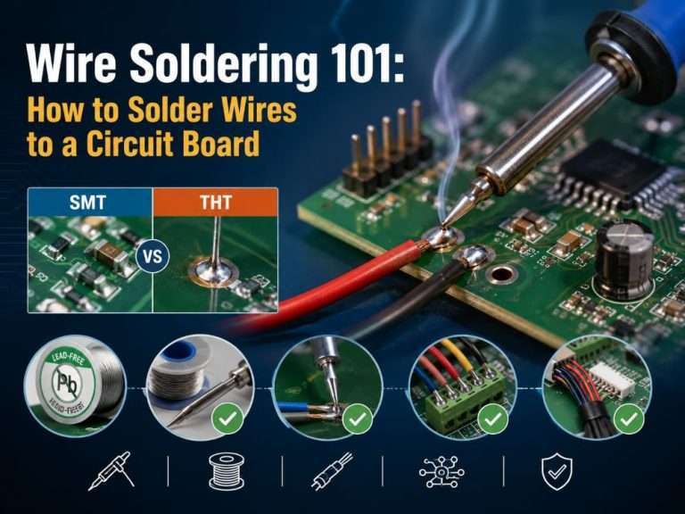
Soldering wire is the fundamental skill in electronics where wire to a プリント基板(PCB). And accuracy ensures reliable partnerships whether you are working professionally, settling a device, or putting together a do-it-yourself project. Thus, using a filler metal solder to unite two or more metal surfaces is known as soldering. In this blog, we will learn how to solder wire to circuit boards.
はんだ線の種類
1. Lead Alloy Solder Wire
最もポピュラーなはんだ線は、金属鉛から製造されたもので、最高級品とされている。スズと鉛の組み合わせが多い。その強固で安定した接着性と接合性から、鉛ベースのはんだは電子機器に最もよく使用されるタイプです。通常190℃で溶融し、40%の鉛と60%の錫でできています。これは、固体から液体への変化の速さを示しています。
2.鉛フリーはんだ
鉛を使用したはんだ線は、長い間、業界の標準であった。しかし、鉛の健康への影響が変化をもたらした。このため、はんだ線の品揃えとコストは数年のうちに大幅に低下した。鉛フリーはんだ線は銅、銀、錫でできている。鉛フリーはんだ線は、鉛入りはんだ線よりも安価である。
鉛フリーはんだ線の融点は217℃から221℃と高い。小型デバイスの削減に役立っている。小さな基板を 鉛フリーはんだ has a few issues. Compared to lead solder wire, they are superior.

Tools and Materials You’ll Need in Wire Soldering
- はんだごて
- ハンダ線
- ワイヤーストリッパー
- はんだ付けされるPCBとワイヤー
- ハンダ付けスタンドまたはサードハンド
- ピンセット(オプション)
- 洗浄用イソプロピルアルコールと糸くずの出ない布
- オプションで、熱収縮チューブや電気テープを使って絶縁することもできる。
ワイヤのはんだ付け手順
ステップ1:ワークスペースの準備
まず、風通しがよく、明るい机が必要です。はんだ付け用のタングルを使用すれば、テーブルを保護し、小さな部品が転がり落ちるのを防ぐことができます。セキュリティーは非常に重要なので、十分な風通しのある場所で作業し、目を保護するためにセキュリティー・グラスの使用を検討すること。
ステップ2:PCBとワイヤーの準備
- PCBを検査する: Now, time to look for any solder pads or through-holes on the PCB. Use isopropyl alcohol to clean these ranges in order to stimulate elimination of clean, oil, or oxidation.
- ワイヤーを剥ぐ: ワイヤーストリッパーを使い、ワイヤーの導体の一部(ほぼ5~10mm)を露出させる。万が一、ワイヤーが撚り線になってしまった場合でも、ほつれを防ぐために撚り線を折り曲げます。
ステップ3:ワイヤーとはんだパッドの錫メッキ
- ティン・ザ・ワイヤー はんだプレスを温め、露出したワイヤーにこて先を接触させる。ワイヤーの先端が触れる部分に少量のはんだを塗ります。はんだがワイヤーを均一かつスムーズに覆うようにする。
- ティン・ザ・パッド Use the tip of the soldering iron to apply a small solder to the PCB padパッド。その後、強力な製本を保証するために、薄くて光沢のあるカバーが必要なだけかもしれない。
ステップ4:ワイヤーをPCBにはんだ付けする
- ワイヤーの位置を決める: ワイヤーは、錫メッキしたパッドの上に置く。必要であれば、ピンセットや第三の手を使って安定させる。
- 熱を加える: 固定プレスの先端をワイヤーとパッドに同時に押し当てる。1~2秒間押し当て、均一に温める。
- Apply Solder: 接合部に直接はんだを塗るのではなく、はんだを送りながら塗る。流れるはんだは、光沢のある円錐形の接合部を形成するはずである。
- 熱を取り除く: 接合部ができたらはんだごてを外し、きちんと冷ます。ワイヤーを移した後、はんだが固まるのを待つ。
ステップ5:作品の検査
はんだの交点をちらっと見ることで、それがきれいで光っていることを確認できます。良い交差点は滑らかで、ワイヤーとパッドをしっかりと覆っているはずです。もし面白みがなかったり、穴があいていたりしたら、加熱してはんだをほんの少し追加してください。
ステップ6:断熱材を入れる(オプション)
熱収縮チューブや電気テープを使って、接続部の近くに露出したワイヤーを保護してください。これにより、意図しない短絡を安全な距離に保つことができます。
ステップ7:接続テスト
最後に、マルチメーターを使ってラッチされた関連付けをテストし、進捗を確認する。これにより、ワイヤーとパッドが合法的に接続されていることが証明される。
機械溶接と手溶接の比較
交換を完了するためにはんだ付けに使用される2つの主要な技術は、機械溶接と手溶接である。
手溶接: この組み合わせは、熟練した専門家が便利なはんだごてを使って行う。この方法は、卓越した柔軟性と汎用性を提供するため、複雑なデザインや魅力的な試みに最適です。
機械溶接: In machine welding, the fastening is done by automated machinery. This makes it unthinkably feasible for large-scale fabrication operations, when consistency and speed are crucial.
Wire Soldering Process for Different PCB Types
単層プリント基板と多層プリント基板では、その構造上の違いから、はんだ付けの手順がまったく異なります。
単層プリント基板のはんだ付け
Soldering techniques for single-layer PCBs are relatively straightforward due to their simple design. With components and traces confined to one layer, ウェーブはんだ付けのようなプロセス または手作業によるはんだ付けが一般的である。
これらの方法は、単層基板の複雑でないレイアウトに効率的であり、迅速な組み立てと必要に応じての手直しが可能である。内部層を考慮する必要がないため、過熱のリスクは最小限に抑えられ、はんだ付け時の単層プリント基板の取り扱いが容易になります。
二層プリント基板のはんだ付け
対照的だ、 多層プリント配線板 require more advanced soldering techniques due to their complex structure of interconnected layers. Reflow soldering is often the preferred method, as it ensures precise and uniform soldering without damaging internal layers.
を使用しています。 ビア and advanced materials in multi-layer boards adds to the complexity, requiring specialized solder and 溶剤 to maintain reliability. Additionally, controlled heating profiles are crucial to prevent thermal damage and ensure strong, defect-free connections across all layers.
ソルダーパッドの種類
THT (Through-Hole Technology) と SMT (Surface Mount Technology) are the two primary types of solder pads, which are necessary for joining 構成要素 to a PCB.
Strong mechanical bonding is provided by THT solder pads, which are perfect for heavy or high-stress components. These pads are made for components with leads that go through holes in the PCB and are soldered on the other side.
SMTはんだ 一方、パッドは平らで、PCB表面に載っている。ピンが短い部品やリード線がない部品に利用され、より小型で軽量な設計を可能にする。
ハンダ付け方法の違い: SMTは、リフローはんだ付けのような精密な方法に依存している。一方、THTでは、穴埋めにより多くのはんだを必要とするウェーブはんだや手はんだが頻繁に使用される。
続きを読む: Difference between SMT and THT.
How to Troubleshoot Common Wire Soldering Problems
コールドソルダー&オーバーヒートジョイント
One particular issue is a cold solder junction, where the solder does not follow well and seems grimy and unclean. This occurs when the component and pads are not sufficiently or evenly warmed. Conversely, overheated joints occur when the PCB or pads becomes overheated, which can lead to the pads lifting off the board.
修正する: By using a fastening press with soldering temperature control and limiting the heat length, this may be prevented.
ブリッジとはんだ不足
Another frequent problem is bridging, in which too much solder creates 短絡回路 between adjacent pads or pins. Lack of solder is another problem that results in a weak connection.
修正する: ブリッジングを修正するには はんだ芯 またはポンプで余分なはんだを取り除く。はんだが足りない場合は、熱の伝わり方を確認しながらはんだを追加することで解決できます。
酸化表面とはんだボール
汚れた表面や酸化した表面には、はんだが付着しない可能性があります。イソプロピル・リカーで洗浄し、フラックスを使用すると、はんだの付着が大幅に向上します。はんだボールは、フラックスの急激な泡立ちや温度ムラによって発生することが多い。
Lifted pads can occasionally occur when the pads separate from the PCB as a result of extreme heat or rough handling. With careful soldering and appropriate temperature control, this may be expected. Misaligned components might also result from poor arrangement or development during fastening.
修正する: 酸化物の表面に光を当てるには、熱を調節して公平に当てること。ピンセットや第三の手を使って部品を安定させることは、直接の和解とみなされる。
はんだジャンパー線はPCBにとって重要か?
基板上の2つの別々の電気回路を接続するワイヤーは、はんだジャンパーワイヤーと呼ばれる。また、はんだを使わずに2つの回路をつなぐ太いワイヤーも含まれる。
連動させると、回路のショートカットとして機能し、ショートする可能性がある。基板上の電気をコントロールすることが可能になる。そのため、配線が少なくて済む基板は、はんだジャンパー線で制御できる。
はんだジャンパー・ワイヤーにはさまざまな色がある。しかし、色はその用途にはほとんど関係ありません。ジャンパー・ワイヤーには、メス端2本、メス端1本とオス端1本、オス端2本の3種類がある。それぞれの端で分離する。メスのはんだジャンパー・ワイヤーは主に接続のために利用されるが、オスのワイヤーの端は突出している。
PCBにワイヤーを取り付ける代替技術
テクニック | メリット | 説明 |
ターミナルブロック |
|
|
コネクター |
|
|
クイックフィックス接着剤 |
|
|
表面実装技術 |
|
|
リフローはんだ付け |
|
|
はんだ工程における安全上のご注意
風通しの良い場所で作業する
特にフラックスや鉛入りはんだを使用する場合は、はんだ付け中に発生するガスを吸い込まないよう、作業スペースを換気よくしてください。
Wear Protective Gear
溶融はんだやフラックスの飛散から目を保護するため、常に安全眼鏡を着用すること。また、火傷から手を守るため、耐熱性の手袋を使用する。
Avoid Direct Contact with Hot Tools
はんだごての先端や加熱された部品に直接触れないこと。部品の取り扱いには、ピンセットやクランプなどの工具を使用してください。
Keep a Clean Workspace
火災の危険を減らすため、作業場所から可燃物を取り除く。より安全なはんだ付けを行うために、整理整頓を心がけてください。
Use a Stable Soldering Iron Stand
はんだごてを使用しないときは、やけどや損傷を防ぐため、必ず安全なスタンドに置いてください。
Unplug When Not in Use
はんだ付けが終わったときや休憩するときは、過熱や事故を防ぐため、はんだごてのプラグを抜いてください。
Wash Hands After Handling Solder
はんだ付けの後は、有害物質への暴露を減らすため、特に鉛入りはんだを使用した場合は、手をよく洗いましょう。
結論
It is important to comprehend the various methods of connecting wires to a PCB in order to design long-lasting and efficient electrical circuits. Depending on the specifications and requirements of your project, you can select the various soldering options. Additionally, the device’s functionality and quality can be significantly impacted by the kind of cable and connector you choose and how you connect them.
よくあるご質問
For most modern PCB electronics, use lead-free rosin-core solder (e.g., SAC305: 96.5% Sn, 3% Ag, 0.5% Cu) with a diameter of 0.6mm (0.023″) to 0.8mm (0.032″). For hobbyists or where regulations allow, 63/37 tin/lead rosin-core (eutectic) is easier to work with and melts at a lower temperature.
The solder wire has a hollow core filled with 溶剤. The flux cleans the metal surfaces (component leads and PCB pads) of oxidation, enabling a strong, reliable bond as you solder.
Fine work (SMD, tight spacing): 0.5mm – 0.6mm
General through-hole components: 0.7mm – 0.8mm
Larger connectors/wires: 1.0mm+
Using solder that’s too thick makes it easy to apply too much and cause bridges.
Lead-Based (Sn63/Pb37): Lower melting point (~183°C), easier to achieve shiny, reliable joints, better “wetting.” Used in hobbyist, aerospace, or メディカル (where allowed). Requires proper ventilation and hygiene.
Lead-Free (e.g., SAC305): Higher melting point (~217-227°C), joints are duller, can be “grittier.” Required for commercial consumer goods by RoHS規制. Needs a slightly hotter iron.
Typically, 2-3 seconds is sufficient. Prolonged heating (more than 3-4 seconds) can lift the copper pad from the PCB (delamination) or damage the component.
お見積もり
関連ブログ
Table of Contents Design Rule Checking in PCB Design: From Altium DRC to SMT Assembly Published on September 10, 2024 · Updated on October 22,
Table of Contents Automotive PCB Assembly: The Complete 2026 OEM Guide Failure of a consumer good is a warranty claim. Failure of an automotive printed
Table of Contents Medical PCB Assembly: The Complete Guide for Medical Device OEMs Medical PCB Assembly is not a commodity process. It is a very
Table of Contents Drone PCB Design and Manufacturing: A Complete Guide for UAV Engineers This article was originally published in March 2024 and last updated
Table of Contents Security Camera PCBA Design Guide: Day/Night Switching and Infrared LED Driver Why Security Camera PCBA Design Matters for Day/Night Operation A security
Table of Contents AgTech Case Study: Manufacturing 2,000+ Agricultural Sensor Devices from Prototype to Production Designing an electronic prototype to large-scale production requires more than