
فهرست مطالب
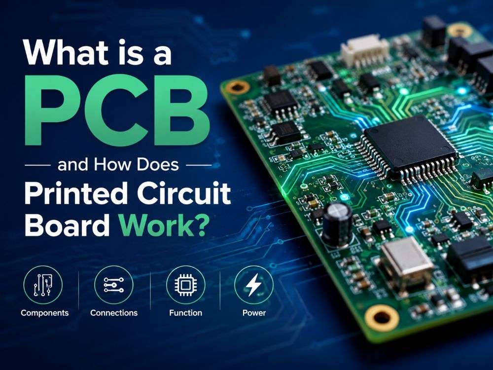
PCB Meaning: What Is a Printed Circuit Board?
This article was originally published in July 2022 and last updated on Sept 10, 2026.

What Does PCB Stand For?
PCB Full Form
- چاپ شده – refers to how circuit patterns are formed on the board.
- Circuit – refers to the electrical paths used to carry power and signals.
- Board – refers to the physical material that supports the circuit.

What Does PCB Mean in Electronics?
برد مدار چاپی چیست؟
- آثار مس are analogous to roads for transmitting signals and power.
- ویاس join the copper paths present at different layers.
- پدها serve as the connection points where the components are soldered.
- Power and ground planes offer broader paths for power transmission and flow of return current.
- قطعات الکترونیکی execute their function of electronics.
What Are the Main Functions of a PCB?
Electrical Interconnection
- قدرت
- Ground
- Digital signals
- Analog signals
- High-speed signals
- Control signals
Mechanical Support

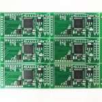
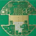
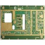
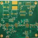

How Does a PCB Work?
					Power Input
     ↓
Power Regulation
     ↓
Microcontroller
     ↓
Sensor / Communication Interface
     ↓
Output Device
What are the Main Parts of a Printed Circuit Board?
| PCB Part | What It Does |
| بستر | Supports the board and provides electrical insulation |
| لایه مس | Forms conductive circuits and planes |
| ردیابی | Carries electrical power or signals |
| پد | Provides a soldering area for components |
| Via | Connects copper layers |
| ماسک لحیم کاری | Protects copper and limits exposed soldering areas |
| سیلک اسکرین | Shows component references and other markings |
| Mounting Hole | Secures the PCB mechanically |
| Ground Plane | Provides a low-impedance electrical return path |
PCB Substrate
Copper Traces
پدها
ویاس
- Through vias
- Blind vias
- Buried vias
- میکروویاس
ماسک لحیم کاری
سیلک اسکرین
- R1, R2, R3 for resistors
- C1, C2, C3 for capacitors
- U1, U2 for ICs
- Connector labels
- Polarity indicators
- Test point identifiers
- Logos
- Warning symbols
PCB Layer Structure Explained
Single-Layer PCB
- LED devices
- Basic appliances
- Simple controllers
- Electronic gadgets of lower complexity

برد مدار چاپی دو لایه

برد مدار چاپی چند لایه
					Top Layer       → Components / Signals
Inner Layer 1   → Ground
Inner Layer 2   → Power / Signals
Bottom Layer    → Components / Signals

What Are the Different Types of PCBs?
| نوع برد مدار چاپی | Main Characteristic | کاربردهای معمول |
| برد مدار چاپی تک طرفه | One copper layer | Simple electronics |
| برد مدار چاپی دو طرفه | Two copper layers | Controllers, power supplies |
| برد مدار چاپی چند لایه | Multiple copper layers | Computers, industrial electronics |
| برد مدار چاپی سفت و سخت | Fixed structure | General electronics |
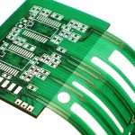
| برد مدار چاپی انعطاف پذیر | Bendable structure | Wearables, cameras |
| PCB سفت و سخت | Rigid and flexible sections | Medical, aerospace |
| برد مدار چاپی HD | High-density interconnection | Smartphones, compact electronics |
| برد مدار چاپی با هسته فلزی | Better heat transfer | LED, power electronics |
برد مدار چاپی سفت و سخت
برد مدار چاپی انعطاف پذیر
PCB سفت و سخت
برد مدار چاپی HD
برد مدار چاپی با هسته فلزی

What Materials Are PCBs Made From?
FR-4
- Electrical isolation
- Mechanical strength
- Heat resistance
- Manufacturing compatibility
- هزینه
High-Frequency PCB Materials
- RF electronics
- Radar systems
- ارتباط بیسیم
- High-speed networking
پلیآمید
Metal Core Materials

Common Components Mounted on a PCB
اجزای غیرفعال
- مقاومتها
- خازنها
- سلفها
اجزای فعال
- Integrated circuits
- Microcontrollers
- ریزپردازندهها
- ترانزیستورها
- دیودها
Connectors and Other Components
- Board-to-board connectors
- Wire-to-board connectors
- USB connectors
- FPC connectors
- Relays
- الایدیها
- حسگرها
- Crystal oscillators
- Switches

PCB vs PCBA: What's the Difference
PCB = bare circuit board. PCBA = assembled circuit board.
| ویژگی | برد مدار چاپی | PCBA |
| Full Meaning | برد مدار چاپی | مونتاژ برد مدار چاپی |
| قطعات | Not populated | Components installed |
| Main Process | ساخت برد مدار چاپی (PCB) | مونتاژ برد مدار چاپی |
| Solder Joints | No component solder joints | بله |
| Electrical Function | Board-level interconnection | Assembled electronic circuit |
| Typical Output | Bare board | Completed assembly |
How is a PCB Manufactured?
طراحی برد مدار چاپی
- قرار دادن قطعات
- Routing
- Layer stack-up
- Board dimensions
- Hole locations
- Electrical clearances
Material Preparation
تصویربرداری مدار
اچینگ
حفاری
Copper Plating
ماسک لحیم کاری
پرداخت سطح
- Lead-Free HASL
سیلک اسکرین
بازرسی و آزمایش

How Are Components Added to a PCB?
SMT — Surface Mount Technology
THT — Through-Hole Technology
- Selective soldering
- Manual soldering
Mixed Technology Assembly
PCB Quality Standards and Testing
بازرسی بصری
- Surface damage
- Solder mask defects
- Exposed copper
- Contamination
- Incorrect markings
- Dimensional problems
AOI
- Missing components
- Incorrect component placement
- Polarity problems
- Solder-related defects
بازرسی با اشعه ایکس
- Bottom-terminated components
- Other hidden solder joints
تست الکتریکی
تست عملکردی
Terms You Need to Know for Basic Circuit Board Design
| Term | تعریف |
| ردیابی | Conductive path carrying electrical signals or power |
| پد | Conductive area used to solder a component |
| Via | Plated connection between PCB layers |
| ردپا | Land pattern that matches a component package |
| Plane | Large continuous copper area |
| Schematic | Electrical representation of a circuit |
| Stack-up | Arrangement of copper and dielectric layers |
| Clearance | Minimum spacing between conductive features |
| خزش | Distance along a surface between conductive points |
| عرض ردیابی | Width of a copper trace |
| اندازه مته | Diameter of a PCB hole |
| وزن مس | Specification related to copper thickness |
| Impedance | Electrical characteristic controlled for certain signal paths |
What PCB Manufacturing Files Do You Need?
فایلهای گربر
- Copper layers
- ماسک لحیم کاری
- سیلک اسکرین
- Board outline
- Other fabrication layers
Drill Files
بوم
- Reference designator
- Manufacturer
- Manufacturer part number
- مقدار
- Component description
- بسته
Pick-and-Place File
- Reference designator
- X/Y coordinates
- Rotation
- Component side
طراحی مونتاژ
What Files Are Needed for PCB Assembly?
- بوم
- Pick-and-place file
- Assembly drawing
- Component information
- Assembly instructions
- Testing requirements
Where Are PCBs Used?
Medical Electronics
- Patient monitors
- Diagnostic equipment
- Portable medical devices
- Imaging systems

الکترونیک خودرو
- Infotainment systems
- Vehicle lighting

Industrial Electronics
- رباتیک
- Industrial sensors
- Automation equipment


Selecting the Correct PCB for Your Application
تعداد لایهها
مواد
ضخامت تخته
ضخامت مس
پرداخت سطح
PCB Technology
- برد مدار چاپی سفت و سخت
- برد مدار چاپی انعطاف پذیر
- PCB سفت و سخت
- برد مدار چاپی HD
- برد مدار چاپی هسته فلزی
Common PCB Problems and Defects
PCB Fabrication Defects
- Open circuits
- Copper peeling
- Delamination
- Solder mask damage
- Incorrect hole dimensions
- Board warpage
- Surface finish defects
PCBA Assembly Defects
- Solder bridges
- سنگ قبرسازی
- Insufficient solder
- Excessive solder
- Component misalignment
- Missing components
- Incorrect component orientation
- Cold solder joints
PCB Manufacturing vs PCB Assembly
تولید PCB
					PCB Design
     ↓
Material Preparation
     ↓
Circuit Formation
     ↓
Drilling
     ↓
Copper Plating
     ↓
Solder Mask
     ↓
Surface Finish
     ↓
Inspection
     ↓
Finished PCB
مونتاژ PCB
					Bare PCB
    +
Electronic Components
     ↓
Solder Paste Printing
     ↓
Component Placement
     ↓
Reflow Soldering
     ↓
THT / Selective Soldering
     ↓
AOI / X-Ray
     ↓
Electrical / Functional Testing
     ↓
Finished PCBA
What is Turnkey PCBA Manufacturing?
تسریع راهاندازی جهانی
با PCBA قابل اعتماد
راه حل یک مرحله ای: ساخت PCB، منبع یابی، مونتاژ SMT، آزمایش و لجستیک جهانی.
چرخش سریع، کنترل کیفیت دقیق.
What Do You Need to Order a PCB or PCBA?
For PCB Manufacturing
- فایلهای گربر
- Drill files
- Board dimensions
- تعداد لایهها
- مواد PCB
- ضخامت تخته
- ضخامت مس
- پرداخت سطح
- Solder mask color
- Required quantity
- Special fabrication requirements
For PCBA Manufacturing
- بوم
- Pick-and-place file
- Assembly drawing
- Component specifications
- Assembly instructions
- Testing requirements
- Special quality requirements
PCB/PCBA RFQ Checklist
| مورد نیاز | ساخت PCB | PCBA Assembly |
| فایلهای گربر | ✓ | ✓ |
| Drill Files | ✓ | ✓ |
| PCB Specifications | ✓ | ✓ |
| بوم | — | ✓ |
| Pick-and-Place File | — | ✓ |
| طراحی مونتاژ | — | ✓ |
| الزامات آزمایش | Optional | ✓ |
| تامین قطعات | — | ✓ / Optional |
نتیجهگیری
Frequently Asked Questions About PCB Meaning
وبلاگ PCB پایه
Table of Contents Design Rule Checking in PCB Design: From Altium DRC to SMT Assembly Published on September 10, 2024 · Updated on October 22,
Table of Contents Automotive PCB Assembly: The Complete 2026 OEM Guide Failure of a consumer good is a warranty claim. Failure of an automotive printed
Table of Contents Medical PCB Assembly: The Complete Guide for Medical Device OEMs Medical PCB Assembly is not a commodity process. It is a very
Table of Contents Drone PCB Design and Manufacturing: A Complete Guide for UAV Engineers This article was originally published in March 2024 and last updated
Table of Contents Security Camera PCBA Design Guide: Day/Night Switching and Infrared LED Driver Why Security Camera PCBA Design Matters for Day/Night Operation A security
Table of Contents AgTech Case Study: Manufacturing 2,000+ Agricultural Sensor Devices from Prototype to Production Designing an electronic prototype to large-scale production requires more than
با FS Technology همکاری کنید، از خدمات حرفهای PCBA بهرهمند شوید