Indice dei contenuti

PCB Meaning: What Is a Printed Circuit Board?

This article was originally published in July 2022 and last updated on Sept 10, 2026.

What is the PCB Meaning in Electronics
PCB is a frequently used term in electronics. But what does PCB actually mean? You’ve probably noticed a green circuit board inside your computer, mobile phone, automotive control module, medical equipment or household appliances and had no idea about its purpose.
 
PCB stands for Printed Circuit Board. It is a physical board with electronic components attached to it that are interconnected using copper traces, pads, vias and other conductive elements.
 
There can be different PCBs – single layer boards or sophisticated multilayer, HDI, flexible and rigid-flex boards. They can be found in various products ranging from consumer electronics and automotive to medical devices and industrial machinery.
 
This guide explains the PCB meaning, how a PCB works, its main parts, PCB types and materials, the PCB manufacturing process, PCB assembly, PCB vs PCBA, basic PCB terms, testing methods, and the information you need when ordering a PCB or PCBA.

What Does PCB Stand For?

PCB Full Form

PCB stands for Printed Circuit Board.
A circuito stampato consists of circuit patterns that are made of conductive materials and some insulating layers. The conductive patterns create the electrical connection, whereas the board serves as a base for the mounting of components.
 
There are three words in the term PCB, and each word describes its basic features:
  • Stampato – refers to how circuit patterns are formed on the board.
  • Circuit – refers to the electrical paths used to carry power and signals.
  • Board – refers to the physical material that supports the circuit.
 
The term “printed” may be deceptive if you try to understand what printing is. PCB manufacturing includes several processes like circuit imaging, etching, drilling, copper plating, solder mask, surface finish and testing.
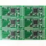
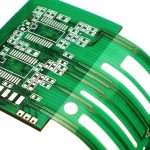
a green bare printed circuit board

What Does PCB Mean in Electronics?

In electronics, the PCB is a platform that connects various components of the circuit.
For example, a controller board may have a microcontroller, resistors, capacitors, sensors, connectors and some interfaces. In order to connect each component with others, wires are not used, and special copper traces are used to make the connection. This process saves space and simplifies the creation of the circuit.

Che cos'è un PCB?

A printed circuit board is a physical structure that serves as a medium to establish electrical connections and structural support for electronic circuits.
 
Usually, a bare PCB does not have the required electronic components for a functional product but is designed to offer the paths, points of connection, insulation, and structure required for them.
Here is one of the simplest ways to understand a PCB and its components:
  • Copper traces are analogous to roads for transmitting signals and power.
  • Vias join the copper paths present at different layers.
  • Tappetini serve as the connection points where the components are soldered.
  • Power and ground planes offer broader paths for power transmission and flow of return current.
  • Componenti elettronici execute their function of electronics.
 
For a simple circuit, the signal path might look like this:
Power Input → PCB Trace → Resistor → IC → LED → Ground
The PCB determines where these connections are located and how power and signals move through the circuit.

What Are the Main Functions of a PCB?

There are two primary functions that a PCB serves – electrical connection e mechanical support.
 

Electrical Interconnection

Copper traces, pads, vias, and copper planes create paths for:
  • Potenza
  • Ground
  • Digital signals
  • Analog signals
  • High-speed signals
  • Control signals
The PCB layout determines how these signals move from one part of the circuit to another.
 

Mechanical Support

It is also responsible for providing mechanical support. Mounting holes and board edges provide the means of installation of the assembled board in the product housing or other mechanical assemblies.
Thus, a PCB is more than just a plain board. The PCB layout, size and manufacturing must all be compatible with the product needs.

How Does a PCB Work?

A PCB works by creating fixed paths for electrical conductivity between the electronic components.
 
Let’s think about an electronic controller as an example. Power flows in through the connector and travels along the copper tracks or power planes. Voltage regulator regulates the voltage to the level needed for this particular circuit. Then, regulated power goes to the MCU and other components.
 
Signals from sensors can flow to the MCU along the signal tracks. Further, after processing the signals, the MCU can send some information to another circuit, display, motor or communication interface.
 
A simple signal path could be represented as follows:
				
					Power Input
     ↓
Power Regulation
     ↓
Microcontroller
     ↓
Sensor / Communication Interface
     ↓
Output Device
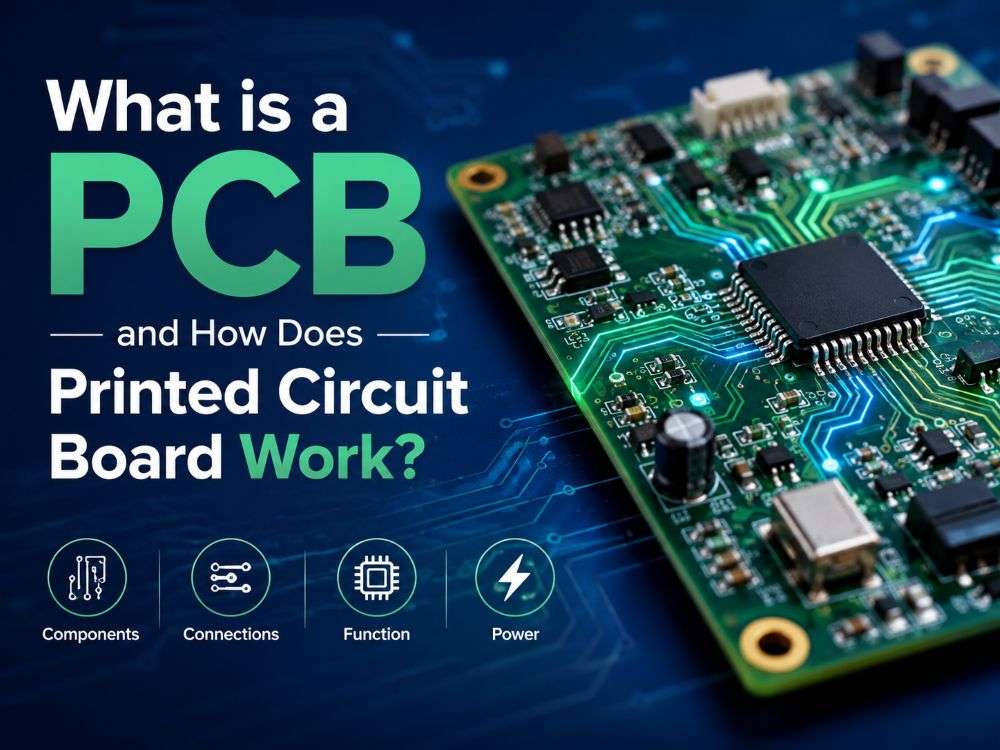
				
			
The PCB is used to create physical connections between the blocks.
 
In case of a simple PCB, routing might be quite straightforward. However, more complicated boards require many additional considerations. For instance, engineers need to think about such things as signal integrity, power integrity, impedance, grounding, gestione termica, EMC and manufacturability.
 
As an example, high speed signal can not always be routed in the same way as a low-speed control signal. Also, high-current power flow might require wider tracks or additional copper layers to manage temperature rise and voltage drop.

What are the Main Parts of a Printed Circuit Board?

Knowing the main PCB parts makes it much easier to understand how a circuit board is designed and manufactured.
PCB PartWhat It Does
SubstratoSupports the board and provides electrical insulation
Strato di rameForms conductive circuits and planes
TracciaCarries electrical power or signals
TamponeProvides a soldering area for components
ViaConnects copper layers
Maschera di saldaturaProtects copper and limits exposed soldering areas
SerigrafiaShows component references and other markings
Mounting HoleSecures the PCB mechanically
Ground PlaneProvides a low-impedance electrical return path

PCB Substrate

Substrate is the primary structural component of the PCB.
For many rigid boards, FR-4 is the default material. It provides an ideal combination of mechanical strength, electrical insulating qualities, thermal properties, and cost.
Other substrates can include polyimide, ceramica, high-frequency laminates, or metal core substrates. The appropriate substrate will depend on the electrical, mechanical, thermal, and environmental conditions of the device.
 

Tracce di rame

Copper traces are the conducting parts of a PCB. They interconnect components and provide a channel to transmit current or signals between various points on the board.
Dimensioning of copper traces should be appropriate to the circuit requirements. Copper trace dimensions like width and thickness will affect the current-carrying capacity, resistivity, temperature rise, voltage drop, and controlled impedance.
A trace carrying a few amps will generally require a different design than one carrying a small-current digital signal.
 

Tappetini

Tappetini are conductive regions in which components are attached to the board.
Surface-mount components use pads on the PCB surface. Through-hole components use pads around drilled holes, and their leads are inserted through the board.
The shape and dimensions of the pads should match those of the component footprints and the selected assembly process.
 

Vias

A via is a plated hole that connects copper planes from one PCB layer to another layer.
This means that signals can originate from one layer, travel to another layer through a via, then to yet another layer through a via, and finally travel back to the first layer through a via.
Types of vias commonly used include:
  • Through vias
  • Blind vias
  • Buried vias
  • Microvias
Vias are most important on multilayer and high-density PCBs where there is limited routing space.
 

Maschera di saldatura

The colored film applied to almost all areas of the PCB is referred to as the maschera di saldatura.
The green color is by far the most popular, although black, blue, red, yellow, white, and any other colors may be used.
The solder mask shields the copper surface and decreases solder bridges during PCB assembly.
 

Serigrafia

Serigrafia refers to the printed marking layer of the PCB. It allows the engineer or technician to locate different points of interest on the PCB.
Examples of markings are:
  • R1, R2, R3 for resistors
  • C1, C2, C3 for capacitors
  • U1, U2 for ICs
  • Connector labels
  • Polarity indicators
  • Test point identifiers
  • Logos
  • Warning symbols
These markings can be useful during assembly, inspection, troubleshooting, and repair.

PCB Layer Structure Explained

Strato PCB count refers to the number of conductive copper layers in the board.
Layer count is determined based on the routing density, power distribution, EMC requirements, space, cost and signal integrity.
 

Single-Layer PCB

A PCB a singolo strato uses a single main copper layer.
This design uses less space for routing; therefore, it is suitable for simpler circuitry.
Examples include:
  • LED devices
  • Basic appliances
  • Simple controllers
  • Electronic gadgets of lower complexity
Che cos'è un PCB a strato singolo?

PCB a doppio strato

A double-layer PCB uses copper on both layers of an insulating substrate.
Vias can link the top and bottom copper layers, allowing designers to have more space to route compared to a single-layer PCB.
Examples of applications for double-sided PCBs include controllers, alimentazione units, industrial, consumer and automotive electronics.
Che cos'è un PCB a doppio strato?

PCB multistrato

A PCB multistrato consists of multiple copper layers separated by dielectric materials.
A basic four-layer PCB might use the following arrangement:
				
					Top Layer       → Components / Signals
Inner Layer 1   → Ground
Inner Layer 2   → Power / Signals
Bottom Layer    → Components / Signals
				
			
More complex products may use 6, 8, 10, 12, or more layers.
However, adding layers does not automatically make a PCB better. The layer count should come from the actual routing, electrical, thermal, mechanical, and manufacturing needs of the design.
Che cos'è un PCB multistrato?

What Are the Different Types of PCBs?

There are different ways of classifying PCBs. Common categories are based on the board structure, flexibility, density, material, and application.
Tipo di PCBMain CharacteristicApplicazioni tipiche
PCB monofaccialeOne copper layerSimple electronics
PCB a doppia facciaTwo copper layersControllers, power supplies
PCB multistratoMultiple copper layersComputers, industrial electronics
PCB rigidoFixed structureGeneral electronics
PCB flessibileBendable structureWearables, cameras
PCB rigido-flessibileRigid and flexible sectionsMedical, aerospace
PCB HDIHigh-density interconnectionSmartphones, compact electronics
PCB con anima in metalloBetter heat transferLED, power electronics
 

PCB rigido

PCB rigido retains its form after fabrication and is the most commonly used in general electronic devices.
It is used in electronic products like control boards, power supplies, computers, household devices, machinery, and automotive electronics.
 

PCB flessibile

PCB flessibile uses bendable materials usually polyimide, and the circuit can bend or follow a bent mechanical structure.
It is useful in cases of space restrictions and moving along with the device.
 

PCB rigido-flessibile

PCB rigido-flessibile makes use of rigid and flexible elements in a single circuit board.
The structure allows reducing cables and separate connector usage. It also allows better fitting electronics in devices with restricted and complex inner space.
 

PCB HDI

High-density interconnects or PCB HDI uses structures like microvias, fine lines, and small features to increase connection density in an area.
It is widely used in compact electronic devices where regular PCB structure is not able to provide sufficient routing space.
 

PCB con anima in metallo

PCB con anima in metallo uses a thermally conductive metallic substrate, usually aluminium, to dissipate heat.
It is widely used in LED illumination and other products where the problem of heat dissipation is very important.

What Materials Are PCBs Made From?

The properties of PCB material have an influence on electrical, mechanical, thermal, reliability and manufacturing cost aspects.
 

FR-4

FR-4 is the most frequently used material for the manufacture of rigid PCBs.
This material provides good characteristics of:
  • Electrical isolation
  • Mechanical strength
  • Heat resistance
  • Manufacturing compatibility
  • Costo
FR-4 is a good material that may be recommended for many ordinary electronic devices.
 

High-Frequency PCB Materials

Special laminates with specific dielectric parameters are necessary for the design of RF and PCB ad alta frequenza.
Such materials are utilized in applications including:
  • RF electronics
  • Radar systems
  • Comunicazione wireless
  • High-speed networking
Material selection becomes more important as signal frequency and data rate increase.
 

Poliammide

Poliammide is widely used in manufacturing flexible PCBs. This material allows flexing and provides heat and electrical properties required for flexible circuit applications.
 

Metal Core Materials

Metal-core PCBs use a conductive metal base to improve heat transfer.
Alluminio is one of the most frequently utilized materials in LED lighting and other devices with thermal performance.

Common Components Mounted on a PCB

A bare PCB becomes a PCBA when componenti elettronici are mounted and soldered onto it.
 

Componenti passivi

Some common examples of passive components are as follows:
  • Resistori
  • Condensatori
  • Induttori
They can be used for current limiting, filtering, energy storage, timing, and signal conditioning.
 

Componenti attivi

Some common examples of active components are as follows:
  • Integrated circuits
  • Microcontrollori
  • Microprocessori
  • Transistor
  • Diodi
For instance, an MCU can read sensor data, perform processing of data, and control other components of the device.
 

Connectors and Other Components

A PCB may also contain:
  • Board-to-board connectors
  • Wire-to-board connectors
  • USB connectors
  • FPC connectors
  • Relays
  • LED
  • Sensori
  • Crystal oscillators
  • Switches
The PCB layout and component selection work together to determine what the final electronic assembly can do.

PCB vs PCBA: What's the Difference

There are similarities between PCB e PCBA, but the two are different.
This is how one can differentiate between the two easily:
PCB = bare circuit board. PCBA = assembled circuit board.
CaratteristicaPCBPCBA
Full MeaningCircuito stampatoAssemblaggio di circuiti stampati
ComponentiNot populatedComponents installed
Main ProcessFabbricazione di PCBAssemblaggio di PCB
Solder JointsNo component solder jointsSì
Electrical FunctionBoard-level interconnectionAssembled electronic circuit
Typical OutputBare boardCompleted assembly
A Produttore di PCB produces the bare board. A Servizio di assemblaggio di PCB adds the components and solders them to the board.
 
The overall process can be viewed as:
PCB → Component Assembly → PCBA → Product Integration
This point is important to keep in mind while asking for a manufacturing quotation. PCB fabrication and PCBA assembly use different equipment, materials, processes, and cost calculations.

How is a PCB Manufactured?

PCB manufacturing turns a digital board design into a physical PCB.
The exact Processo di produzione dei PCB varies with the board type and required technology, but a typical process includes the following steps.
 
  1. Progettazione di PCB

Engineers create the schematic and Layout del PCB using electronic design automation software.
The design defines items such as:
  • Posizionamento dei componenti
  • Instradamento
  • Layer stack-up
  • Board dimensions
  • Hole locations
  • Electrical clearances
  1. Material Preparation

The selected copper-clad laminate is prepared according to the required material, thickness, and layer structure.
  1. Circuito di imaging

Il schema del circuito is transferred onto the relevant copper layer.
  1. Incisione

Unwanted copper is removed to leave the required conductive pattern.
  1. Perforazione

Mechanical or laser drilling creates holes for vias, through-hole components, mounting points, and other requirements.
  1. Copper Plating

Copper plating forms the required electrical connections through drilled holes and between PCB layers.
  1. Maschera di saldatura

A solder mask coating is applied to protect the copper and leave the required soldering areas exposed.
  1. Finitura superficiale

Exposed copper receives a finitura superficiale. Common options include:
The right finish depends on the board design, component package, reliability requirements, assembly process, and budget.
  1. Serigrafia

Reference markings, polarity information, and other board information are printed onto the PCB.
  1. Ispezione e test

The finished board can go through visual inspection, dimensional checks, electrical testing, and other quality checks based on the project requirements.

How Are Components Added to a PCB?

Assemblaggio di PCB is the process of mounting electronic components onto a fabricated PCB.
There are two main types of assembly: SMT e THT.
 

SMT — Surface Mount Technology

With SMT technology, surface-mount components are soldered directly to the solder pads of the board.
A typical Processo SMT is:
Solder Paste Printing → SPI → Pick and Place → Reflow Soldering → SMT AOI
Assemblaggio SMT suits automation and allows placing many tiny components in a small space.
 

THT — Through-Hole Technology

Through-hole components feature leads which are soldered to the holes in the PCB.
According to the board and component, THT components may be soldered by means of:
Assemblaggio THT is usually applied for large connectors, power components, relays, and other components requiring higher mechanical strength.
 

Mixed Technology Assembly

In modern PCBA manufacturing, there are many assemblies with both SMT and THT, which are called mix-technology assembly.
For instance, the controller board could have hundreds of small SMT parts and some big connectors or through-hole parts.
Consequently, it is necessary for the Produttore di PCBA to examine the entire BOM, PCB design, part packages, and assembly process prior to manufacturing.

PCB Quality Standards and Testing

Sometimes, even an ideal-looking PCB could have hidden electrical or manufacturing issues which will be very difficult to detect by eye. Quality checks and testing help find these issues before the board reaches the customer.
 

Ispezione visiva

Ispezione visiva can identify problems such as:
  • Surface damage
  • Solder mask defects
  • Exposed copper
  • Contamination
  • Incorrect markings
  • Dimensional problems
 

AOI

Ispezione ottica automatizzata (AOI) utilizes cameras and inspection software to inspect PCB assemblies.
It can detect issues such as:
  • Missing components
  • Incorrect component placement
  • Polarity problems
  • Solder-related defects
 

Ispezione a raggi X

Ispezione a raggi X is very useful for checking solder joints which could not be examined using non-destructive optical methods.
It is widely used for:
  • Bottom-terminated components
  • Other hidden solder joints
 

Test elettrici

Electrical testing can detect open circuits, shorts and other electrical connections issues.
Common methods include:
 

Test funzionali

Test funzionali examines whether a produced PCBA meets all its operational requirements.
For instance, power boards could be tested for output voltage and current, while a communication board should establish the required connection and perform the data exchange properly.
The test plan depends on the product and its risk level.

Terms You Need to Know for Basic Circuit Board Design

PCB terminology may seem complex initially when dealing with circuit boards. The terms below include most of the basics that you would encounter while designing circuit boards.
TermDefinizione
TracciaConductive path carrying electrical signals or power
TamponeConductive area used to solder a component
ViaPlated connection between PCB layers
ImprontaLand pattern that matches a component package
PlaneLarge continuous copper area
SchematicElectrical representation of a circuit
Stack-upArrangement of copper and dielectric layers
ClearanceMinimum spacing between conductive features
StrisciaDistance along a surface between conductive points
Larghezza della tracciaWidth of a copper trace
Dimensione della puntaDiameter of a PCB hole
Peso del rameSpecification related to copper thickness
ImpedenzaElectrical characteristic controlled for certain signal paths
These terms come up quite often in circuit board designs, manufacturing processes, Analisi DFM, and conversations between engineers and PCB suppliers.

What PCB Manufacturing Files Do You Need?

Accurate data about your circuit board will help the supplier understand your design and save you from additional questions during manufacturing. The following are 5 essential PCBA manufacturing files you should provide to the PCB manufacturer.
 

File Gerber

File Gerber represent the graphical data required to manufacture each layer of the PCB.
They may include:
  • Copper layers
  • Maschera di saldatura
  • Serigrafia
  • Board outline
  • Other fabrication layers
 

Drill Files

Drill files include information about the positions and sizes of holes on the circuit board.
They are necessary for vias, through-hole parts, mounting holes, etc.
 

BOM

A Distinta dei materiali (BOM) lists the components needed for PCB assembly.
A typical BOM may contain:
  • Reference designator
  • Manufacturer
  • Manufacturer part number
  • Quantità
  • Component description
  • Pacchetto
 

Pick-and-Place File

Pick-and-place file gives automated assembly equipment the information needed to place components.
It commonly contains:
  • Reference designator
  • X/Y coordinates
  • Rotation
  • Component side
 

Assembly Drawing

Assembly drawing provides additional information about the position of components, orientation, polarity, etc.
 

What Files Are Needed for PCB Assembly?

For bare PCB fabrication, Gerber files and drill files are normally the key production files.
Per Assemblaggio PCBA, the manufacturer will generally also need:
  • BOM
  • Pick-and-place file
  • Assembly drawing
  • Component information
  • Assembly instructions
  • Testing requirements
A complete data package makes it easier to review the design, check DFM issues, prepare production, and calculate the quotation.

Where Are PCBs Used?

Medical Electronics

Medical equipment may use PCBs in:
Medical applications can have increased quality control, traceability, testing and manufacturing requirements.

Elettronica per autoveicoli

Since automotive electronics can operate in a range of temperature conditions, vibration, electrical transients, and extended operational periods, their PCB materials, components, design, and manufacturing should correspond to the automotive environment.

Industrial Electronics

Industrial boards may be subjected to vibrations, temperature changes, electrical noise, and long operational periods.

Selecting the Correct PCB for Your Application

While selecting a PCB may entail choosing between a two-layer and four-layer PCB, there are other important considerations.
 

Conteggio degli strati

The number of layers must be in harmony with the routing density, power delivery, signal integrity, EMC and the complexity of the circuits.
Over-use of unnecessary layers will not solve any problem but increase the cost of the board.
 

Materiale

For most of the products FR-4 would do, high-frequency, flexible, high-temperature, and heat dissipation designs might need other types of material.
 

Spessore del pannello

Spessore del PCB affects mechanical strength, enclosure fit, connector design, and in some designs, impedance.
 

Spessore del rame

Copper thickness affects current capacity, resistance, and heat generation.
Power boards often require thicker copper than low-current control boards.
 

Finitura superficiale

The surface finishing must be compatible with the component type, required reliability, assembly process, storage conditions and budget.
 

PCB Technology

Depending on the product, you may need:
  • PCB rigido
  • PCB flessibile
  • PCB rigido-flessibile
  • PCB HDI
  • PCB con anima in metallo
The proper PCB is the one which will satisfy all of your product’s requirements without unnecessary expense and complication.

Common PCB Problems and Defects

Having knowledge about common defects in PCBs can be helpful for both engineers and purchasing agents for easier understanding of production problems and more effective communication with PCB suppliers.
 

PCB Fabrication Defects

Common defects in the PCB fabrication process include:
  • Open circuits
  • Copper peeling
  • Delamination
  • Solder mask damage
  • Incorrect hole dimensions
  • Board warpage
  • Surface finish defects
Some of these defects may cause electrical failure, and some other may become mechanical or reliability-related problems.
 

PCBA Assembly Defects

Common defects in the Processo di assemblaggio PCBA includono:
  • Solder bridges
  • Lapide
  • Insufficient solder
  • Excessive solder
  • Component misalignment
  • Missing components
  • Incorrect component orientation
  • Cold solder joints
 
It is useful to separate PCB fabrication defects from PCBA assembly defects.
A bare PCB can be manufactured correctly but still develop an assembly problem during component placement or soldering. On the contrary, the PCBA process can be done without errors even if there are defects in the fabricated PCB.

PCB Manufacturing vs PCB Assembly

Produzione di PCB e Assemblaggio di PCB are connected, but they are two different processes.

Produzione di PCB

The goal is to produce the bare PCB:
				
					PCB Design
     ↓
Material Preparation
     ↓
Circuit Formation
     ↓
Drilling
     ↓
Copper Plating
     ↓
Solder Mask
     ↓
Surface Finish
     ↓
Inspection
     ↓
Finished PCB


Assemblaggio di PCB

The goal is to turn the bare PCB into an assembled PCBA:
				
					Bare PCB
    +
Electronic Components
     ↓
Solder Paste Printing
     ↓
Component Placement
     ↓
Reflow Soldering
     ↓
THT / Selective Soldering
     ↓
AOI / X-Ray
     ↓
Electrical / Functional Testing
     ↓
Finished PCBA


What is Turnkey PCBA Manufacturing?

A turnkey PCBA service combines several production steps through one manufacturing company:
PCB Manufacturing → Approvvigionamento dei componenti → SMT/THT Assembly → Inspection → Testing → Delivery
 
It is convenient for foreign clients to buy and manage production in one place. It means that you need not communicate with many companies for PCB manufacturing, component procurement, assembly, and testing.
🌍 Scheda elettronica globale · Soluzione chiavi in mano

Accelerare il lancio globale
con PCBA affidabile

One-stop solution: PCB fabrication, sourcing, SMT assembly, testing & global logistics.
Tempi di consegna rapidi, controllo qualità rigoroso.

⚡ Consegna rapida in 5-7 giorni 🏭 ISO13485 / IATF16949 ✈️ Spedizione in tutto il mondo
Contatto →
⏱️ Consulenza specialistica 24 ore su 24, 7 giorni su 7

What Do You Need to Order a PCB or PCBA?

Before requesting a quotation, prepare the engineering and manufacturing information required for the project.

For PCB Manufacturing

You should generally provide:
  • File Gerber
  • Drill files
  • Board dimensions
  • Conteggio degli strati
  • Materiale del PCB
  • Spessore del pannello
  • Spessore del rame
  • Finitura superficiale
  • Solder mask color
  • Required quantity
  • Special fabrication requirements
 

For PCBA Manufacturing

In addition to the PCB files, provide:
  • BOM
  • Pick-and-place file
  • Assembly drawing
  • Component specifications
  • Assembly instructions
  • Testing requirements
  • Special quality requirements
 

PCB/PCBA RFQ Checklist

RequisitiFabbricazione di PCBAssemblaggio PCBA
File Gerber✓✓
Drill Files✓✓
PCB Specifications✓✓
BOM-✓
Pick-and-Place File-✓
Assembly Drawing-✓
Requisiti per i testOptional✓
Approvvigionamento di componenti-✓ / Optional
The more complete the manufacturing data is, the easier it is for a supplier to review the project, identify possible DFM problems, and prepare an accurate quotation.

Conclusione

So, what does PCB mean?
PCB means Printed Circuit Board. It offers the physical connectivity that enables electronic parts to get powered up, communicate signals, and function as an integrated unit.
 
There are various types of PCBs ranging from simple single-layer to more complex multi-layer, HDI, flex, rigid-flex and high-frequency PCBs.
Knowledge on the meaning of PCB, PCB layers, materials, components, traces, vias, surface finishes, manufacturing process, PCB assembly, and PCB testing forms a good platform to start working on your electronic hardware.
 
However, creating a reliable electronic product requires more than just manufacturing a PCB. Additional steps in some projects might include component sourcing, SMT & THT assembly, inspection, electrical test, functional test, production quality control, etc.
 
If you are looking for a manufacturing partner for PCB fabrication, PCB assembly, or turnkey PCBA manufacturing, an experienced PCBA supplier can help take your project from engineering files to finished production.
Need help with your next PCB or PCBA project? Contact our engineering team for manufacturing support and a customized quotation.

Frequently Asked Questions About PCB Meaning

PCB stands for Circuito stampato. It is a board with conductive structures used to connect and support electronic components.
PCB meaning in electronics refers to a Circuito stampato, the physical platform used to connect components and carry power and signals through copper traces, pads, vias, and planes.
A PCB is normally the bare circuit board, while a PCBA is a PCB populated with electronic components and soldered to form an assembled electronic circuit.
The main PCB parts include the substrate, copper layers, traces, pads, vias, solder mask, silkscreen, and mounting holes.
Common PCB types include single-sided, double-sided, multilayer, rigid, flexible, rigid-flex, HDI, and metal-core PCBs.
FR-4 is widely used for rigid PCBs. Other materials include polyimide, high-frequency laminates, ceramic, and metal-core materials.
A PCB works by providing conductive paths between electronic components. Copper traces, pads, vias, and planes carry power and signals according to the circuit design.
Components are mainly mounted using SMT (Surface Mount Technology) o THT (Through-Hole Technology). Many PCB assemblies use both methods.
PCB manufacturing is the process of producing a bare circuit board from a digital design. It can include circuit imaging, etching, drilling, copper plating, solder mask application, surface finishing, silkscreen printing, inspection, and testing.
PCB assembly is the process of mounting and soldering electronic components onto a fabricated PCB to create a PCBA.
The right PCB depends on the product’s electrical, mechanical, thermal, environmental, and manufacturing requirements. Key factors include layer count, material, thickness, copper weight, surface finish, PCB technology, and reliability requirements.

Blog sui PCB di base

Collabora con FS Technology e ottieni un servizio professionale di assemblaggio di schede elettroniche (PCBA).