
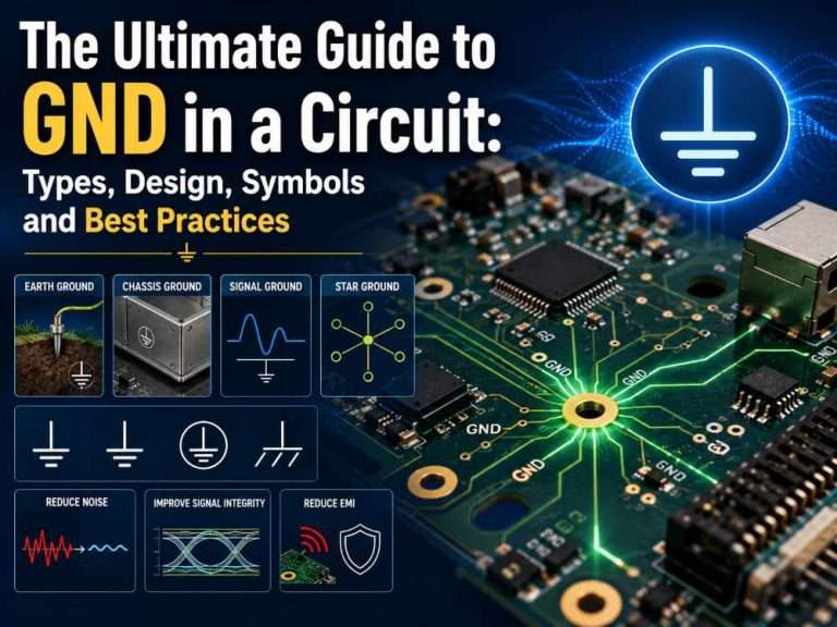
The Ultimate Guide to GND in a Circuit: Types, Design, Symbols and Best Practices
Введение
GND в цепи представляет собой общую точку, через которую электрический ток возвращается к источнику. В случае, если ток не возвращается, GND может в буквальном смысле спасти жизнь. Для большинства производителей электроники актуальным вопросом является Что такое внутрисхемный GND?
Что такое GND в цепи?

Принцип работы цепи GND In Circuit
Why is GND in Circuit so Important?
- Voltage Reference Point: Voltages refer to a potential difference, and all measurements are taken from a reference point. The ground plane or net is usually identified as the reference point at 0 V. Voltages of +3.3 V are then referenced from the ground plane or GND.
- Current Return Path: All outgoing current must return to its source in accordance with the current continuity path principle. The main current return path from both signal and power current is through the GND. An important professional design consideration is that current return path needs to have low impedance and good control because it affects signal integrity and EMC performance.
Типы GND в цепи
Для различных применений используется несколько типов GND. Наиболее распространенными являются заземление, шасси и сигнальное заземление, но мы рассмотрим больше из них.
Заземление (EGND)
Заземление шасси
Сигнальная земля (SGND)
Аналоговая земля (AGND)
Цифровая земля (DGND)
Заземление питания (PGND)
Заземление переменного тока (CGND)
Star Ground
Плавающее основание
Critical Conceptual Clarifications of GND in Circuit
GND vs. AGND (Analog Ground)
- Relation: AGND stands for a particular subset of the total GND system. In schematics, “GND” symbolizes the generic term, whereas “AGND” represents the isolated area earmarked for analog devices in the mixed-signal PCB layout.
- Distinction: The general ground network can introduce noise, while AGND is designed to behave noiselessly. The manner in which these grounds are coupled together, frequently through a single point of connection or star point, represents an important design trade-off in eliminating ground noise issues in analog circuits.
GND (Circuit Ground) vs. Earth Ground
- Key Difference: Circuit GND is an electrical reference point, a local “0V” that can be floating. Grounding can refer to the connection of electrical devices to the earth in terms of safety aspects.
- Functional Difference: It works using the internal GND of the circuit. In most circuits, when current flows, it does not go through the Earth. The chassis of the circuit is attached to the Earth for safety.
GND vs. Power Supply Negative (-) Terminal
- Role Definition: GND represents the reference plane of the system, while the Power Supply Negative represents an Energy return port.
- Practical Application:
- In single supply circuits, such as +5 V supplies, the negative lead is usually considered the system ground; essentially, they are the same.
- In a dual-supply or bipolar supply system (for example, ±12 V), the ground (GND) is fixed at the midpoint between the two supplies. It is not the same as V- or V+ terminals.
Is GND Positive or Negative?
- Core Principle: The polarity of GND is relative because it depends upon its role in the system.
- Analysis:
- In a positive-supply-only system, GND denotes the most negative point and the lowest potential.
- In a negative-supply-only system, GND symbolizes the maximum potential or the most positive point.
- In a bipolar supply system, GND is the reference between the two.
- Заключение: GND itself is neither positive nor negative; it is referenced as the 0-volt reference point, and all other points in the circuit are labeled as positive or negative relative to GND.

Professional GND Implementation in PCB Design
Grounding Methodologies
- Single-Point Grounding: Used in low-frequency analog designs (< 1MHz). It eliminates ground loops and common-impedance noise by grounding all ground points at a single point.
- Multi-Point Grounding & Ground Planes: These are necessary in high-frequency digital and RF designs above 10 MHz. Ground planes offer the lowest possible impedance return path, reduce the area of loops, and offer shielding in addition; these are the standards of today’s Высокоскоростные конструкции.
- Hybrid Grounding: Used in mixed-signal circuits, where analog ground (AGND) and digital ground (DGND) are interconnected at a single point. It ensures that there is no noise coupling, but at the same time, it maintains the high-frequency return path.
Core Design Principles
- Keep Low Impedance: Solid ground planes are preferred whenever possible; wide следы can be employed for power grounds.
- Control Return Currents: Think about the return path of the high-speed signals, usually under the signal trace. Don’t cut or moat through the return path.
- Manage Currents: Keep high-noise power return current paths away from low-noise signal return current paths, and layout the PCB so that there are no shared ground paths.
Mechanisms of Common GND-Related Problems
- Common-Impedance Coupling:It happens when both circuits share the same ground trace segment. Noise current from the “noisy” circuit (e.g., a digital IC) causes a corresponding voltage drop in the shared impedance, which manifests as an error signal in the “quiet” circuit (e.g., a sensor).
- Ground Bounce: In digital VLSI circuits, the inductance due to package leads or bonds can cause ground bounce when many outputs change at the same time (e.g., a data bus), resulting in logical errors and increased EMI.
- Ground Loops: Form when a system is grounded at multiple points, creating a large loop area. Alternating magnetic fields can induce circulating currents in this loop, which manifest as hum (50/60 Hz) or other noise in sensitive analog signals.
Как устранить неполадки с GND
Заключение
FAQs about GND in Circuit
Мы будем рады услышать от Вас
Похожие блоги
Table of Contents Precision Agriculture – How IoT PCBA Is Transforming Modern Farming Precision agriculture is transforming modern farming by combining IoT sensors, wireless connectivity,
Table of Contents PCB Meaning: What Is a Printed Circuit Board? This article was originally published in July 2022 and last updated on Sept 10,
Table of Contents Smart Lighting Control PCBA: Comprehensive Engineering Guide for Zigbee 3.0 Dimming and SCR Compatibility Creating the Smart Lighting Control PCBA, which is
Table of Contents Custom PCB Design and Manufacturing: A Comprehensive Guide for Engineers and Product Developers This article was originally published in Mar 2024 and
Table of Contents How to Read a Circuit Board: A Complete Step-by-Step Guide for Engineers and Technicians (2026) Printed Circuit Board Assemblies (PCBAs) form the
The Ultimate Guide to WiFi Extenders: Technology, Market Trends, and PCBA Manufacturing Insights Think about this: you are conducting an important video conference, and then