
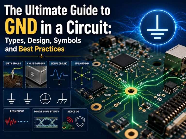
The Ultimate Guide to GND in a Circuit: Types, Design, Symbols and Best Practices
Introduzione
Il GND in un circuito rappresenta un punto comune in cui la corrente elettrica ritorna alla sorgente. Nel caso in cui la corrente non ritorni, il GND può letteralmente salvare delle vite. Una domanda pressante della maggior parte dei produttori di elettronica è Che cos'è il GND in circuito?
Che cos'è il GND nel circuito?

Principio di funzionamento del circuito GND In
Why is GND in Circuit so Important?
- Voltage Reference Point: Voltages refer to a potential difference, and all measurements are taken from a reference point. The ground plane or net is usually identified as the reference point at 0 V. Voltages of +3.3 V are then referenced from the ground plane or GND.
- Current Return Path: All outgoing current must return to its source in accordance with the current continuity path principle. The main current return path from both signal and power current is through the GND. An important professional design consideration is that current return path needs to have low impedance and good control because it affects signal integrity and EMC performance.
Tipi di GND nel circuito
Per le varie applicazioni si utilizzano diversi tipi di GND. I più comuni sono le masse di terra, di telaio e di segnale, ma ne esamineremo altri.
Terra (EGND)
Massa del telaio
Massa del segnale (SGND)
Massa analogica (AGND)
Massa digitale (DGND)
Massa di alimentazione (PGND)
Massa CA (CGND)
Terra delle stelle
Terreno galleggiante
Critical Conceptual Clarifications of GND in Circuit
GND vs. AGND (Analog Ground)
- Relation: AGND stands for a particular subset of the total GND system. In schematics, “GND” symbolizes the generic term, whereas “AGND” represents the isolated area earmarked for analog devices in the mixed-signal PCB layout.
- Distinction: The general ground network can introduce noise, while AGND is designed to behave noiselessly. The manner in which these grounds are coupled together, frequently through a single point of connection or star point, represents an important design trade-off in eliminating ground noise issues in analog circuits.
GND (Circuit Ground) vs. Earth Ground
- Key Difference: Circuit GND is an electrical reference point, a local “0V” that can be floating. Grounding can refer to the connection of electrical devices to the earth in terms of safety aspects.
- Functional Difference: It works using the internal GND of the circuit. In most circuits, when current flows, it does not go through the Earth. The chassis of the circuit is attached to the Earth for safety.
GND vs. Power Supply Negative (-) Terminal
- Role Definition: GND represents the reference plane of the system, while the Power Supply Negative represents an Energy return port.
- Practical Application:
- In single supply circuits, such as +5 V supplies, the negative lead is usually considered the system ground; essentially, they are the same.
- In a dual-supply or bipolar supply system (for example, ±12 V), the ground (GND) is fixed at the midpoint between the two supplies. It is not the same as V- or V+ terminals.
Is GND Positive or Negative?
- Core Principle: The polarity of GND is relative because it depends upon its role in the system.
- Analysis:
- In a positive-supply-only system, GND denotes the most negative point and the lowest potential.
- In a negative-supply-only system, GND symbolizes the maximum potential or the most positive point.
- In a bipolar supply system, GND is the reference between the two.
- Conclusione: GND itself is neither positive nor negative; it is referenced as the 0-volt reference point, and all other points in the circuit are labeled as positive or negative relative to GND.

Professional GND Implementation in PCB Design
Grounding Methodologies
- Single-Point Grounding: Used in low-frequency analog designs (< 1MHz). It eliminates ground loops and common-impedance noise by grounding all ground points at a single point.
- Multi-Point Grounding & Ground Planes: These are necessary in high-frequency digital and RF designs above 10 MHz. Ground planes offer the lowest possible impedance return path, reduce the area of loops, and offer shielding in addition; these are the standards of today’s progetti ad alta velocità.
- Hybrid Grounding: Used in mixed-signal circuits, where analog ground (AGND) and digital ground (DGND) are interconnected at a single point. It ensures that there is no noise coupling, but at the same time, it maintains the high-frequency return path.
Core Design Principles
- Keep Low Impedance: Solid ground planes are preferred whenever possible; wide tracce can be employed for power grounds.
- Control Return Currents: Think about the return path of the high-speed signals, usually under the signal trace. Don’t cut or moat through the return path.
- Manage Currents: Keep high-noise power return current paths away from low-noise signal return current paths, and layout the PCB so that there are no shared ground paths.
Mechanisms of Common GND-Related Problems
- Common-Impedance Coupling:It happens when both circuits share the same ground trace segment. Noise current from the “noisy” circuit (e.g., a digital IC) causes a corresponding voltage drop in the shared impedance, which manifests as an error signal in the “quiet” circuit (e.g., a sensor).
- Ground Bounce: In digital VLSI circuits, the inductance due to package leads or bonds can cause ground bounce when many outputs change at the same time (e.g., a data bus), resulting in logical errors and increased EMI.
- Ground Loops: Form when a system is grounded at multiple points, creating a large loop area. Alternating magnetic fields can induce circulating currents in this loop, which manifest as hum (50/60 Hz) or other noise in sensitive analog signals.
Come risolvere i problemi di GND
Conclusione
FAQs about GND in Circuit
Saremo lieti di ascoltarvi
Blog correlati
Table of Contents Design Rule Checking in PCB Design: From Altium DRC to SMT Assembly Published on September 10, 2024 · Updated on October 22,
Table of Contents Automotive PCB Assembly: The Complete 2026 OEM Guide Failure of a consumer good is a warranty claim. Failure of an automotive printed
Table of Contents Medical PCB Assembly: The Complete Guide for Medical Device OEMs Medical PCB Assembly is not a commodity process. It is a very
Table of Contents Drone PCB Design and Manufacturing: A Complete Guide for UAV Engineers This article was originally published in March 2024 and last updated
Table of Contents Security Camera PCBA Design Guide: Day/Night Switching and Infrared LED Driver Why Security Camera PCBA Design Matters for Day/Night Operation A security
Table of Contents AgTech Case Study: Manufacturing 2,000+ Agricultural Sensor Devices from Prototype to Production Designing an electronic prototype to large-scale production requires more than