目次

The Ultimate Guide to GND in a Circuit: Types, Design, Symbols and Best Practices
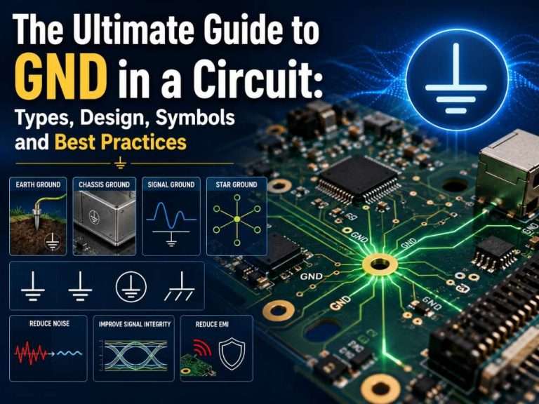
What is GND in Circuit

はじめに

回路のGNDは、電流がソースに戻る共通点を表す。電流が戻らない場合、GNDは文字通り命を救うことになる。多くの電子機器メーカーが抱える切迫した問題は GNDインサーキットとは?

Ground, or “GND” in electronic design terminology, is considered an essential but rather misunderstood element in many electronic designs. Being referred to as “the zero-volt connection” in many definitions, Grounding covers far more than most designs understand. Inadequate grounding design can result in anything from stray noises and signal degradation to persistent electromagnetic interference (EMI) in an electronic design and even complete failure.
 
FSテック offers a thorough analysis of GND, moving beyond basic definitions in examining the role of GND as a hierarchical structure, clarify common misconceptions, and outline professional design and debugging practices in this blog.

回路のGNDとは?

電気用語でGNDはアースを意味する。私たちが立っているグラウンドのことではありません。このグランドは、PCB上のすべての電圧の基準点となる。電流は負荷から信号を受け取った後、回路を流れます。グランドまたはGNDは、その電流が戻るための経路を提供します。
 
When you turn on a TV, it sends a signal to request power from the source so it can operate. The current follows the path determined by the circuit, powers the TV, and returns to the source. You must be wondering what the GND does during this process.
 
ここで、GNDは銅製のワイヤーである、 アルミニウムまたはスチール。障害が発生するまでは電流を流さない。電流がその経路から外れると、この電線は安全にそれを大地に放電し、潜在的な損害や危険を防ぎます。これが、通常アース線と呼ばれる理由である。
GND symbols

GNDイン回路の動作原理

GND(接地)の概念は、19世紀に地球が電気信号の帰還経路を提供できることに人類が気づいたときに生まれた。ドイツの科学者カール・アウグスト・フォン・シュタインハイルが最初に電信機でこれを試み、当時はかなりの人気を博した。しかし、時が経つにつれ、いくつかの問題が表面化してきた。
 
The GND connection is supposed to be low-resistance to guide the current back to the source. However, prolonged dry weather in that era reduced the ground’s moisture. This increased GND’s resistance and stopped the current from flowing back. Signals and communication suffered a lot on a regular basis.
 
やがて、電信に代わって電話が普及し始めた。都市は拡大し、より多くの電線や通信線が敷設された。人間の電磁波活動はすべて、地球内に不要な電流の海を作り出した。この海や誘導電流は、信号を妨害するノイズを発生させ、おそらく永遠に妨害し続けるだろう。
 
これが、電子システムにおいてGNDが重要な理由である。PCB内のすべての部品は、GNDのおかげで本来の動作をします。電流は、GNDを介してすべてのコンポーネントを流れた後、電源で始まり、電源で終わります。このGND接続がなければ、回路は不完全なものとなり、電子システムは動作しなくなる。

Why is GND in Circuit so Important?

GNDは、回路の機能性、安定性、安全性の理由です。障害や突然のサージが発生した場合、電流を大地に放電することにより、機器やユーザーを潜在的な危険から保護します。
 
PCB、電源システム、通信機器において、アースは非常に重要です。アース、シャーシ、信号、またはその他の実行可能なアースを使用して、安全で信頼性の高い電子システムを構築する機会を提供します。
 
The following is where GND serves two indispensable functions in any electronic system:
 
  1. Voltage Reference Point: Voltages refer to a potential difference, and all measurements are taken from a reference point. The ground plane or net is usually identified as the reference point at 0 V. Voltages of +3.3 V are then referenced from the ground plane or GND.
  2. Current Return Path: All outgoing current must return to its source in accordance with the current continuity path principle. The main current return path from both signal and power current is through the GND. An important professional design consideration is that current return path needs to have low impedance and good control because it affects signal integrity and EMC performance.

GND回路の種類

GNDは様々な用途に使われる。最も一般的なものはアース、シャーシ、シグナル・グラウンドであるが、ここではさらに多くのものを見ていくことにする。

アースグランド(EGND)

EGND は、今日の電気システムで最も広く使われているタイプの接地である。金属棒、プレート、リングなどの接地電極を使用して、システムを実際の大地に接続する。これらの電極は、以下のような導電性の高い材料で構成されている。 銅亜鉛メッキ鋼、ステンレス鋼、銅被覆鋼。
 
接地電極は、構造物の電気パネル近くの地下に埋設されている。GNDは接地導線を介して接地電極に接続され、接地導線は同じパネル内の接地バスに接続される。
 
住宅、オフィス、工場など、ほとんどすべての都市構造物にはEGNDがある。EGNDは、障害電流が地面に放電する安全な経路を提供することによって、これらの建物を衝撃や火災から保護する。

シャーシ・グラウンド

EGNDへの接続は、用途によっては必ずしも可能ではない。例えば、携帯電子機器や 自動車 常にアースに接続されている。アースに接続するのは、電源やバッテリーが切れたときだけだ。battery.
 
In such cases, a ground plane is used as the common reference point. A ground plane on a PCB or GND PCB is a large copper layer on the board. It acts as a reference for all the electricity flowing across the board. It means that the metal structure of the device itself (car, mobile phone, or laptop) becomes the GND.
 
があります。 chassis ground シャーシグランドは、デバイスの動作に影響を与える電磁干渉(EMI)からシステムを保護します。グラウンドに直接接続されているわけではありませんが、デバイスのコンポーネントや人体から余分な電流を遠ざけています。

シグナル・グラウンド(SGND)

SNGD は、デバイス間を移動する信号の基準点となる。各デバイスには電源があるため、その電圧は多少異なることがある。このわずかな差が、ノイズを発生させ信号を歪ませる小さな電流を生み出す。SNGDは、このようなノイズ電流から信号経路を分離する。
 
You can use signal ground in pcb which heavily depends on signal processing. For example, PCBs in sound systems need SGND to stop electrical signals from interfering with the audio signals. Signal ground isolates the noise so you can hear clear sound.

アナログ・グラウンド(AGND)

エレクトロニクスには、アナログとデジタルの2種類の信号がある。アナログ信号はゆっくりとした連続的な信号であるのに対し、デジタル信号は瞬間的な電気信号である。高速のデジタル信号がアナログ信号と衝突すると、アナログ信号の品質は低下する。
 
It requires a proper circuit board ground to split the paths of analog and digital signals. You can create AGND by specifying a point on an analog circuit to serve as a reference. It prevents digital noise from interfering with analog signals.

デジタル・グラウンド(DGND)

Digital Ground(DGND) is a reference for high-speed digital signals and manages the noise created by their quick switching. It keeps them separate from disrupting analog signals, so systems with mixed-signal integrated circuits (ICs) can run smoothly.
 
Analog components like ADCs (Analogue-to-Digital Converters) and DACs (Digital-to-Analog Converters) provide an interface between analog signals and digital processes. For example, many 医療機器 monitor analog signals like heartbeat and convert them to digital data for diagnosis.
 
デジタル・ノイズは、このような敏感なアナログ信号に混入し、不正確な測定値を引き起こす可能性があります。そのため、DGNDで接地する必要がある。

電源グランド(PGND)

PGND は、PCB の電源回路と大電流コンポーネントのグランドポイントである。このタイプのグラウンドは、アナログ信号を妨害する電源回路からのノイズを絶縁する。EGNDと同様、電気的な障害が発生した場合に電流の通り道を確保する。すべてのコンポーネントが1つの基準点を共有するように、さまざまな電源電圧を接続する。
 
また、導体を接地電極に接続することでPGNDを作ることもできる。余分な電流を大地に安全に放散することで、機器や人間を感電から守ります。PGNDが正しく実装されていれば、不規則な電圧変動を調整することができます。

ACグランド(CGND)

CGND の交流電流(AC)の基準点である。 AC-DC電源 回路に接続される。通常、インダクタ(L)またはカップリング・コンデンサ(C)を使用してDCグラウンドに接続される。DC信号を遮断することで、ACの通過を助ける。
 
Cは、交流周波数に対して低抵抗で、直流に対して高抵抗のハイパス・フィルターである。2つの回路ノードの間に配置すると、直流部分を分離し、交流のみを伝送することができる。
 
多くのエンジニアは、信号がドロップする可能性を最小限に抑えるために、Cを信号源の近くに配置する。Cはまた、Lと一緒にLCフィルターを形成するために使用することもできる。これにより、特定の周波数をフィルタリングし、他の周波数を通過させるグラウンドの能力が倍増する。

スターグラウンド

このタイプの接地は、複数のGNDを星形の1点に接続する。この設計により、PCB PCB部品 が互いに干渉しないようにする。複数の高周波導体を近接させると、EMIはICのクロストークの原因となる。
 
コモン・グラウンドPCBのようなものです。すべての部品が1つのGNDを共有することで、回路の異なる部分間の干渉を防ぎ、電圧が変動しないようにする。

フローティング・グラウンド

実際のアースから絶縁された回路内のすべての電圧の基準点である。ほとんどの電子機器はプリント基板にGNDを備えており、これはグランドに接続されていることを意味する。しかし、このアースへの接続が実装されていない場合、グラウンドは「浮いている」と言われる。
 
多くのアプリケーションにおいて、機器をアースに接続することは重大な危険を引き起こす可能性があります。大地は、負荷の故障や自然災害によって高電圧を伝える可能性があります。このような状況では負荷にサージが発生し、機器や人体にダメージを与える危険性があります。
 
GNDを絶縁することで、回路は独立して動作し、繊細な機器を保護することができる。フローティング・グラウンドは、負荷電流を正確に測定するための手段として説明されることが多い。これはGNDの一種ではなく、GNDに問題がある場合に適用する条件に過ぎない。

Critical Conceptual Clarifications of GND in Circuit

GND vs. AGND (Analog Ground)

  • Relation: AGND stands for a particular subset of the total GND system. In schematics, “GND” symbolizes the generic term, whereas “AGND” represents the isolated area earmarked for analog devices in the mixed-signal PCB layout.
  • Distinction: The general ground network can introduce noise, while AGND is designed to behave noiselessly. The manner in which these grounds are coupled together, frequently through a single point of connection or star point, represents an important design trade-off in eliminating ground noise issues in analog circuits.

GND (Circuit Ground) vs. Earth Ground

  • Key Difference: Circuit GND is an electrical reference point, a local “0V” that can be floating. Grounding can refer to the connection of electrical devices to the earth in terms of safety aspects.
  • Functional Difference: It works using the internal GND of the circuit. In most circuits, when current flows, it does not go through the Earth. The chassis of the circuit is attached to the Earth for safety.

GND vs. Power Supply Negative (-) Terminal

  • Role Definition: GND represents the reference plane of the system, while the Power Supply Negative represents an Energy return port.
  • Practical Application:
    • In single supply circuits, such as +5 V supplies, the negative lead is usually considered the system ground; essentially, they are the same.
    • In a dual-supply or bipolar supply system (for example, ±12 V), the ground (GND) is fixed at the midpoint between the two supplies. It is not the same as V- or V+ terminals.

Is GND Positive or Negative?

  • Core Principle: The polarity of GND is relative because it depends upon its role in the system.
  • Analysis:
    • In a positive-supply-only system, GND denotes the most negative point and the lowest potential.
    • In a negative-supply-only system, GND symbolizes the maximum potential or the most positive point.
    • In a bipolar supply system, GND is the reference between the two.
  • 結論 GND itself is neither positive nor negative; it is referenced as the 0-volt reference point, and all other points in the circuit are labeled as positive or negative relative to GND.
回路内GND

Professional GND Implementation in PCB Design

Grounding Methodologies

  • Single-Point Grounding: Used in low-frequency analog designs (< 1MHz). It eliminates ground loops and common-impedance noise by grounding all ground points at a single point.
  • Multi-Point Grounding & Ground Planes: These are necessary in high-frequency digital and RF designs above 10 MHz. Ground planes offer the lowest possible impedance return path, reduce the area of loops, and offer shielding in addition; these are the standards of today’s 高速設計.
  • Hybrid Grounding: Used in mixed-signal circuits, where analog ground (AGND) and digital ground (DGND) are interconnected at a single point. It ensures that there is no noise coupling, but at the same time, it maintains the high-frequency return path.

Core Design Principles

  • Keep Low Impedance: Solid ground planes are preferred whenever possible; wide 痕跡 can be employed for power grounds.
  • Control Return Currents: Think about the return path of the high-speed signals, usually under the signal trace. Don’t cut or moat through the return path.
  • Manage Currents: Keep high-noise power return current paths away from low-noise signal return current paths, and layout the PCB so that there are no shared ground paths.

Mechanisms of Common GND-Related Problems

  • Common-Impedance Coupling:It happens when both circuits share the same ground trace segment. Noise current from the “noisy” circuit (e.g., a digital IC) causes a corresponding voltage drop in the shared impedance, which manifests as an error signal in the “quiet” circuit (e.g., a sensor).
  • Ground Bounce: In digital VLSI circuits, the inductance due to package leads or bonds can cause ground bounce when many outputs change at the same time (e.g., a data bus), resulting in logical errors and increased EMI.
  • Ground Loops: Form when a system is grounded at multiple points, creating a large loop area. Alternating magnetic fields can induce circulating currents in this loop, which manifest as hum (50/60 Hz) or other noise in sensitive analog signals.

GND問題のトラブルシューティング方法

GNDには、接続不良やグラウンドループなど、いくつかの問題がある可能性がある。これらの問題を解決する一つの方法は、接地導体に損傷の兆候がないかチェックすることである。メンテナンスや修理が適時に行われないと、適切なGND接続ができなくなる。
 
Next, check if all bonds (bonding connections) throughout the PCB and other circuits are reinforced or replaced (if broken). Regularly test ground fault circuit interrupters (GFCIs) to check if they’re automatically disconnecting power whenever there’s a fault. These practices can prevent serious damage to man and machine.
 
There are several techniques to measure and trace the exact spot of the issue in GND. You can use a resistance meter, a circuit tracer, or an ohmmeter. Resistance meter is to check the resistance from the positive to negative points. A safe value would be somewhere between 0.5 to 2 ohms.
 
また、回路トレーサーを使って、回路に信号を送り、それを受信することで、GND経路に沿った問題を検出することもできます。オーム計は、問題を引き起こしている回路を正確に特定するのに役立ちます。

結論

The knowledge of electronic design involves understanding the hierarchical nature of GND, distinguishing between its conceptual representations, and practicing the low-impedance, controlled-return current path on a PCB. It can all begin by stepping away from the simplistic definition of GND as simply 0 V and recognizing its existence as a basic reference and return ground. With such understanding, effective high-performance, compliant, and robust electronic designs can be developed.
 
費用対効果の高いサービスを提供 PCBアセンブリサービス お客様のビジネスニーズに合わせて 今すぐパートナーになる プロジェクトの目標を達成するために。

FAQs about GND in Circuit

In a single-supply system, yes, the negative terminal is typically defined as the system GND. However, in systems with bipolar supplies (e.g., ±12V), GND is an independent reference point between the positive and negative rails.
We separate them to prevent the high-frequency, noisy currents from the digital circuitry from flowing through the same copper as the analog ground, which would corrupt the sensitive analog reference voltage and degrade performance.
A solid ground plane minimizes the impedance of return paths, which helps. However, ground loops can still form at a larger system level—for example, when two grounded devices are connected by a cable. The resulting large loop area can still pick up interference.
This often points to a missing or poor Earth ground connection. The bench supply may be floating, while the wall adapter connects to Earth. This change can create ground loops or alter the common-mode operating point of your circuit. Always ensure your chassis is properly connected to Earth.

ぜひ、ご意見をお聞かせください

関連ブログ