
Solar Panel PCB: Innovations Driving Efficiency and Sustainability

Introduzione
With the growth of solar technology, there has also been a huge growth in the requirement for new solutions that will advance the capabilities of solar panels and make them more affordable and dependable. This demand has given rise to breakthroughs in the design and functionality of Solar PCBs.
FS Tech’s specialist procurement team is dedicated to sourcing the best raw materials for the manufacture of solar panels. Contattateci today for all your business needs!
What is a Solar PCB?
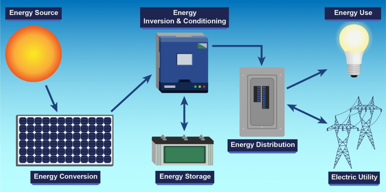
Now, we will easily know what a Solar PCB is. It is a special printed circuit board designed purposely for systems of solar power with the use of structural and electrical elements necessary for harnessing solar energy.
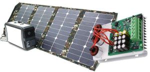
Comparison Between Solar PCBs and Traditional PCBs
In the conventional solar system, sunlight is processed by photovoltaic cells, which in turn produce direct current (DC). This is then sent to the Solar PCB, which routes it through a network of pathways and components designed to deliver maximum power.
Rather than designing normally printed circuit boards, which are found in many electronic devices, the Solar PCB’s features are purely designed to withstand harsh environments while maximizing energy conversion.
Caratteristica | Traditional PCB | Solar PCB |
Primary Application | General Electronics | Solar Energy Systems |
Temperature Resistance | Moderato | Alto |
Environmental Durability | Limitato | Enhanced for outdoor and extreme conditions |
Key Components | Standard Electrical Parts | PV Cells, MPPT Controllers, Charge Controllers |
Efficiency Focus | Not specialized | Optimized for Solar Energy Conversion |
The Structure of Solar PCBs
Solar PCBs are normally made up of different layers of materials, each serving a different function that together guarantees efficiency and stability in the solar system.
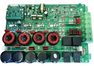
- Substrato materials: Solar PCB substrates are usually manufactured with high heat- and UV-resistant materials, normally FR4, or even more advanced ones like PTFE and Rogers materials that can maintain stable performances in extreme climatic conditions.
- Conductive Layer: The conductive layer consists of copper foil on the PCB, which develops circuit alignments and connections. The width and thickness of the copper foil will be designed such that the current requirement of the circuit is minimal to avoid resistance and thereby heat generation.
- The insulating layers: The insulation is around and between the conductive layers to prevent possible short circuits between them. These usually comprise the usual insulation materials like FR4 or PTFE and provide the required electrical isolation.
- Thermal Management Structures: Solar PCBs are designed to handle thermal management, including thermal vias and thermal pads, which assist in conducting heat from the inside of the board to the outside to maintain the component’s operating temperature.
- Surface treatment: Since the solar PCB needs to improve solder quality and corrosion resistance, some special trattamenti superficiali should be adopted, such as immersion gold, OSP, hard gold, or argento ad immersione.
Importance of Solar PCBs
PCB solar panels use the photovoltaic effect to generate electricity. They are thin and portable, highly efficient and integrated, low cost, highly reliable, and widely used. With technological progress, the photoelectric conversion efficiency will improve, the cost will be reduced, and the application areas will be expanded, which will help the global energy transition and sustainable development.
Enhanced Energy Conversion Efficiency
Durability in Harsh Environments
Cost-Effectiveness and Scalability
Environmental Sustainability
Applications of Solar PCBs
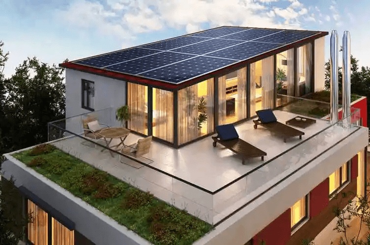
Residential Solar Power Systems
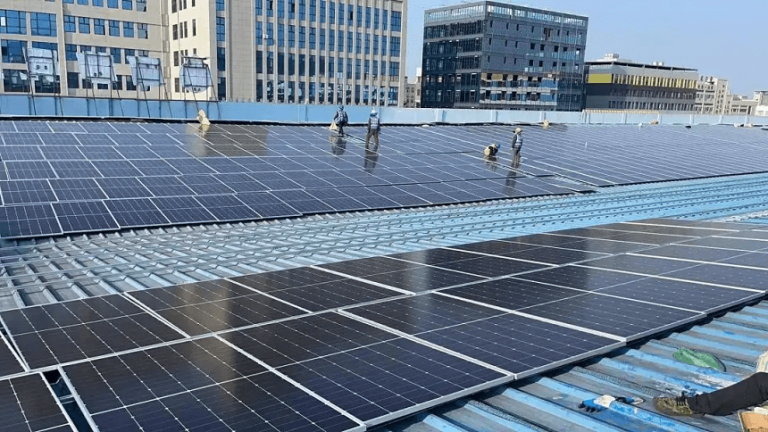
Commercial and Industrial Installations
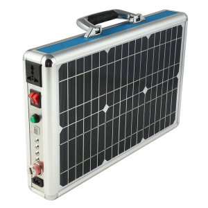
Portable Solar Devices
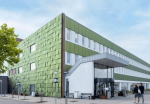
Integrated Solar Architecture
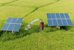
Agriculture
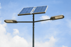
Solar-Powered Street Lightin
Design Considerations for Solar PCBs
- Efficienza – To achieve the best possible energy conversion to energy output, the number of photovoltaic (PV) cells, the physical layout, and interconnection among the circuitry are done in such a manner so that resistance and power loss are at their lowest. With such configurations, solar panel circuit boards can be expected to have minimal losses in solar energy as they transmit energy.
- Dissipazione del calore – In practice, solar PCBs will likely be installed for long durations in direct sunlight. This invariable fact leads to the generation of heat. Certain measures of restraining heat such as heat sinks or high thermal mass materials are effective in controlling thermal loads hence reducing operational temperatures for effective protection of the components from damage.
- Durata – Since solar PCBs are used outdoors, they have to withstand environmental conditions such as UV rays, water, and temperatures. Such durability is important for boards solar light circuit boards and MPPT circuit boards so that they can be able to operate efficiently for years under different environmental conditions.
Solar PCB Manufacturing
Do you remember how to make a PCB, FS Tech discussed it in a previous blog, if you don’t you can review it. Well, the manufacturing process for Solar PCBs is a similar step-by-step process.
Step 1: Circuit Layout
The first step of the design stage is the circuit layout to make sure energy flow is maximized. This design describes the electrical current path, and it is specifically designed in such a way that energy losses are at a minimum.
Step 2: Material Selection
The material that is selected has good quality, is UV stable, and is heat resistant for it to endure the outside environments. These materials augment the resilience of the solar circuit boards against abiotic stresses, and hence, the form and function are preserved.
Fase 3: posizionamento dei componenti
Critical parts are Photovoltaic cells and MPPT controllers, and their position is emphasized as they are placed where their performance will be maximized. Placement is important to efficiency since power systems have each component that must be controlled and harnessed at the right place and time.
Step 4: Assembly and Soldering
The components are assembled and soldered onto the board, making it a single structure. This procedure is important in the construction of solar inverter PCBs and solar panel circuit boards that can withstand high power loads without loss of reliability.
Step 5: Quality Control and Testing
Achieving Technical Innovation in Solar PCBs
Advancements in Photovoltaic Cell Technology
Integration of Smart Sensors and IoT
Development of Flexible and Lightweight Solar PCBs
Conclusione
Saremo lieti di ascoltarvi
Blog correlati
Table of Contents Design Rule Checking in PCB Design: From Altium DRC to SMT Assembly Published on September 10, 2024 · Updated on October 22,
Table of Contents Automotive PCB Assembly: The Complete 2026 OEM Guide Failure of a consumer good is a warranty claim. Failure of an automotive printed
Table of Contents Medical PCB Assembly: The Complete Guide for Medical Device OEMs Medical PCB Assembly is not a commodity process. It is a very
Table of Contents Drone PCB Design and Manufacturing: A Complete Guide for UAV Engineers This article was originally published in March 2024 and last updated
Table of Contents Security Camera PCBA Design Guide: Day/Night Switching and Infrared LED Driver Why Security Camera PCBA Design Matters for Day/Night Operation A security
Table of Contents AgTech Case Study: Manufacturing 2,000+ Agricultural Sensor Devices from Prototype to Production Designing an electronic prototype to large-scale production requires more than