
Automotive-Grade Manufacturing and Thermal Cycling Testing of ECU (Engine Control Unit) PCBA
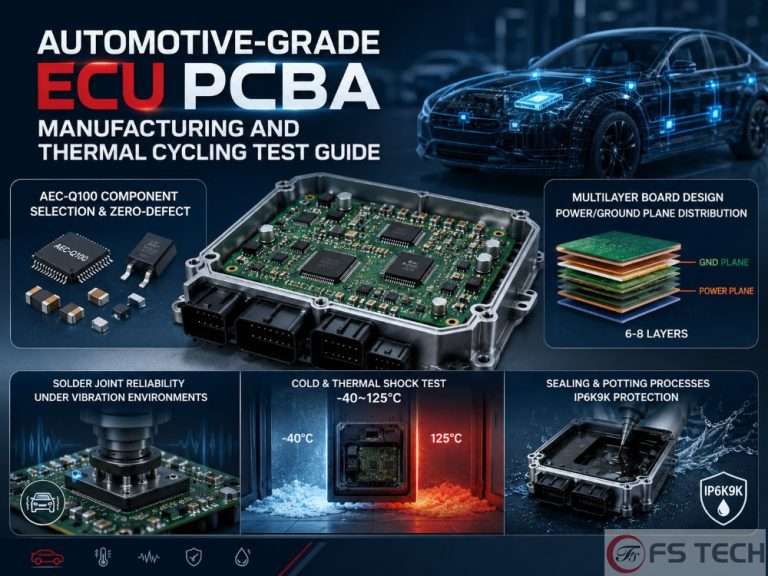
Component Selection: AEC-Q100 and Zero-Defect Framework
What is AEC-Q100?
- Grade 0 (-40°C to 150°C): It contains Engine bay, transmission control units, and turbocharger actuators.
- Grade 1 (-40°C to 125°C): It contains standard under-hood environments and high-power cabin applications.
- Grade 2 (-40°C to 105°C): It contains passenger cabin electronics and infotainment.
- Grade 3 (-40°C to 85°C): It contains basic cabin accessories.
How to Achieve Zero-defect Automotive ECU PCBA Manufacturing?
- Part Average Analysis (PAT): The Statistical tool that identifies and eliminates outliers from a wafer lot is called PAT. Even if an item passes the normal electrical tests, if its performance characteristics are sufficiently different from the statistical average of the remainder of the batch, it will be flagged and thrown away.
- Strict Traceability: All components of an automotive-grade PCBA are laser marked with a unique identifier that traces back to the manufacturing lot, wafer ID, and assembly shift. When a field failure occurs, the engineers are able to trace the error back to the particular silicon ingot from which it is derived. This will allow the company to conduct targeted recalls of just those vehicles containing the defective silicon, rather than a major recall of all the vehicles as happened in earlier cases.
Multilayer PCB Design: 6 to 8-Layer Stackups

Distribution of Ground and Power Plane of a 6 Layer PCB
- Layer 1 (Top Component / Signal): High-speed digital signals, microcontrollers, low-power passives.
- Layer 2 (Ground Plane): A continuous sheet of solid copper ground plane. The reference return path for high-frequency signals above Layer 1 is served by this component.
- Layer 3 (Power / Signal): Low-frequency signals and auxiliary power rails (3.3V, 5V).
- Layer 4 (Power Plane): It is for dedicated distribution of power (12V battery power, high- current driver rails).
- Layer 5 (Ground Plane 2): A continuous ground plane provides reference and shielding to the bottom.
- Layer 6 (Bottom Signal): The routing of high-current switching components, power MOSFETs, and external connector pins driver signal of Layer 6.
Layout Strategies for Automotive EMC
- The copper layout should be centered in the horizontal center plane of the board. An asymmetrically designed stackup results in irregular stress distribution when going through thermal cycling. The result is warping of the board (bow and twist) during assembly reflow and under-hood operation.
- The routing and construction of signal traces must ensure that the traces do not make a cross at any place on their underlying reference plane. When this happens, a large current loop area is generated. This functions as a loop antenna that can radiate high-frequency noise and fail emissions tests.
- Thermal Vias underneath Power ICs. High-current driver ICs and PMICs generate a significant amount of localized heat. The attached thermal vias have to be placed underneath the thermal pads of these components so that there are no thermal hotspots. These vias will suck heat from the top layer and spread it to the inner solid copper ground and power planes.
Automotive ECU PCBA Manufacturing Process Flow

Solder Joints Reliability: Vibration and Thermal Stress
How thermal stress (-40°C to 125°C) work
- Where α is the CTE of the material. Let’s examine how this disappointment manifests itself in real life.
- CKT and FR4 Substrates have an in-plane CTE (X-Y axis) of 14 to 18 ppm/∘C.
- Ceramic chip components, such as MLCC capacitors, have a CTE of 5 to 7 ppm/∘C.
- Silicon ICs such as Microcontrollers have a CTE of 3 ppb/°C
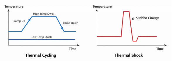
Thermal Cycling vs. Thermal Shock Testing
- Thermal Cycling: The PCB assembly is maintained in a chamber, and the air temperature is increased and decreased at an average rate of 10 ∘C to 15 ∘C per minute. The board stands at the extreme temperatures of −40∘C and +125∘C for a period of 30 minutes. Motor vehicle specifications widely seek a PCBA that can withstand between 1 and 2000 cycles without a broken open circuit in any of them.
- Thermal Shock: Thermal shock testing is another much more aggressive test. The printed circuit board assembly switches from -40 ∘C to 125 ∘C in a relatively quick time frame. The temperature ramp rate is limited to over 30∘C/min due to the near-instantaneous transfer speed. Consequently, large localized mechanical shocks are initiated in the components and their solder structures, rapidly revealing embedded manufacturing flaws.

Solder Degradation Mechanisms
- IMC (intermetallic compounds) growth refers to the formation of tin-copper intermetallic layers (Cu6Sn5 and Cu3Sn) during the リフローはんだ付けプロセス (reaction of solder tin with PCB copper pad). A robust metallurgical bond requires this layer. But too much exposure to high temperatures (125∘C) will cause this IMC layer to become too thick. Due to the brittleness of IMCs, large thicknesses cannot sustain vibration due to structural weakness.
- Melting of solder often exhibits a phenomenon called solder creep. When subjected to constant stress (for example due to CTE mismatch at high temperatures), it will deform permanently over time, a process known as creep.
- During thermal cycling, microcracks start appearing in the region of high stress concentration, which are generally at the corners of the component termination. These slow cracks will extend in the solder joint of the component and make a complete break in the connection.
Sealing and Potting: IP6K9K Protection
Engineering Trade-offs in Potting
| プロパティ | エポキシ樹脂 | Polyurethane (PU) Resins | Silicone Resins |
| Durability of Materials | Very high; superb vibration damping. | Adaptable; adjustable. | Soft and gel-like, low. |
| Heat Resistance | Suitable for temperatures up to 150∘C. | Keeps warm to 120°C. | Good up to 200∘C+ |
| CTE Correspondence | Unyielding; can cause stress on precision SMD components. | Versatile; accommodates slight discrepancies. | High flexibility; causes little stress on its components. |
| Water-resistant. | Great | Very Good | Impressive |
- Silicones & Polyurethanes: Used for engine-mounted ECUs due to their flexibility. They absorb stress during thermal cycling without cracking.
- Epoxies: Offer excellent structural protection but are rigid. During thermal cycling, they can expand and contract, tearing fine-pitch IC pins off the PCB.
結論
グローバル展開を加速する
信頼性の高いPCBAを使用
One-stop solution: PCB fabrication, sourcing, SMT assembly, testing & global logistics.
迅速な対応、厳格な品質管理。.
FAQs about Automotive ECU PCBA
- The zero-defect targets for web interfaces are quality levels in the parts per billion (PPB) rather than parts per million (PPM). They are designed for a life in excess of 15 years under the harshest of conditions.
- Manufacturers must subject every integrated circuit to AEC-Q100 stress testing as defined by the manufacturer (usually Grade 1 or Grade 0 for high-temperature under-hood environments).
- EMI Containment: They give dedicated solid ground planes to shield the high-speed processor lines from noisy power circuits.
- Symmetric multilayer stackups: Symmetric multilayer stackups prevent the board from warping (bowing/twisting) during high-temperature manufacturing and during operational heat cycles.
- Thermal Cycling: The temperature is changed at a speed of about 10 C/min for long-term fatigue and solder joint wear tests.
- Test number: thousands of cycles.
- Thermal shock: Thermal shock forces components from one temperature to another (over 30 C/min) to create strain in the part and immediately reveal latent design or manufacturing defects.
- Vibrations and thermal expansion inside a vehicle can easily crack standard solder.
- Innolot and similar alloys introduce elements such as Bismuth, Antimony, and Nickel that enhance the metal matrix, preventing micro-cracking and solder joint failure.
FSテクノロジーと提携して、プロフェッショナルなPCBAサービスを手に入れましょう。
関連ブログ
Table of Contents Design Rule Checking in PCB Design: From Altium DRC to SMT Assembly Published on September 10, 2024 · Updated on October 22,
Table of Contents Automotive PCB Assembly: The Complete 2026 OEM Guide Failure of a consumer good is a warranty claim. Failure of an automotive printed
Table of Contents Medical PCB Assembly: The Complete Guide for Medical Device OEMs Medical PCB Assembly is not a commodity process. It is a very
Table of Contents Drone PCB Design and Manufacturing: A Complete Guide for UAV Engineers This article was originally published in March 2024 and last updated
Table of Contents Security Camera PCBA Design Guide: Day/Night Switching and Infrared LED Driver Why Security Camera PCBA Design Matters for Day/Night Operation A security
Table of Contents AgTech Case Study: Manufacturing 2,000+ Agricultural Sensor Devices from Prototype to Production Designing an electronic prototype to large-scale production requires more than