
High Speed Printed Circuit Board Manufacturing and Assembly
What are high speed PCBs?
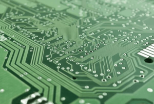
High-Speed PCB Design Features
- Is the impedance controlled on this circuit board? The result will determine whether the board is a signal-ended circuit or differential.
- At what impedance is the controlled impedance circuit running? g., the answer may be 90, 100, or 120 ohms.
- Where is the location for the application of high-speed PCB? As using high-speed.
- Closer to the power line or noisy part of the circuit results in poor signal operation and?
Signal Integrity | Signal integrity is critical to maintaining high-frequency signals on high-speed PCBs. It ensures that the signal reaches its destination without any distortion. |
Impedance Control | Characteristic impedance is the ratio of the voltage amplitude and current of a single wave propagating over a transmission line. In the case of characteristic impedance or surge impedance, the impedance of one transmission line must not affect the other. |
Return Paths | There must be a sufficient number of unified grounding to achieve effective routing. There must be minimal or no gaps between the ground and power layers, as routing high transmission lines through these gaps can be challenging. |
Thermal Management | High-speed circuits generate too much heat, reducing signal performance and damaging components. Proper thermal management ( e.g., heat sink ) is critical to ensure the reliable operation of high-speed PCBs. |
Differential Signaling | Differential signaling uses two complementary signals instead of one to transmit high-speed signals. This method can reduce the common mode noise and ensure the minimum deviation between signals. |
Simulation and Analysis | High-speed PCB designs require careful analysis and simulation to ensure signal integrity and reliability. Simulation tools can be used to model circuit behavior and spot potential problems before the board is manufactured. |
High-Speed PCB Manufacturing Considerations

- Stack Up Development: It is important to ensure proper layer stacking, which makes the foundation layer on which designs are built. It should be carefully observed when selecting laminate materials, dielectric properties, and copper weights based on the required speed characteristics.
- Drilling: In the drilling process, the holes are then drilled in the layers by a drill, machinery-based and computer-controlled.
- Plating: There is a specific chemical solution to help mount the layers when the circuit is set for plating. After plating, we clean the circuit board by applying different chemicals. This seeps into the drilled holes.
- Outer Layer Imaging: The next step in manufacturing a high-speed printed circuit board is applying a photoresist layer to the outermost layer. The UV lights make the photoresist hard.
- Impedance control: The correct calculation of the required impedance values should be considered first. Consistent impedance saves unwanted reflections that corrupt the data. We can control impedance in high-speed Printed circuit boards by using advanced calculators to dial in trace dimensions depending on stack-up properties.
- Etching: The chemical solutions used before are used to remove unwanted copper found below the resist layer. this enables the PCB connection.
- Solder Mask: This is the last stage of the high-speed PCB manufacturing process. The manufacturer must clean all the panels and board before soldering mask implementation. A solder mask can help make the connections stronger on the PCB board. And what we obtain after soldering is the green color of the PCB.
Role of High-Speed PCB in Blinding Pace of Progress
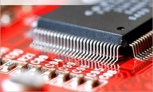
Accelerating Success with High-Speed PCB

High Speed Printed Circuit Board Assembly
In a marketplace intensely hungry for speedier solutions, verified prototypes build confidence and unlock funding for new product initiatives. Yet realizing high performance depends wholly on fabrication and assembly competence. The PCB fabrication process itself demands extraordinary precision. Final boards won’t perform as designed if unduly influenced by production variability or defects. Only thoroughly validated, high-quality components can ensure reliable functionality for proof-of-concept testing rather than distorting results. Most printed circuit boards are considered a signal integrity risk associated with high-speed digital designs. Some factors should be considered during the high-speed PCB assembly process.
- Component Placement
- Applications
- Troubleshooting Circuit Board
- Testing & Inspection
- Final Assembly
The Never-Ending Journey Of High Speed PCB
High-performance PCB design, manufacturing, and unyielding iteration now live at the heart of electronics innovation as data demands intensify. As artificial intelligence, 5G telecommunications, high-performance computing, and big data continue propelling exponential progress, printed circuit boards must keep pace every step of the way. Comprehensively mastering signal integrity and impedance control principles will future-proof products for the blistering speeds of tomorrow. With battle-tested design software, trusted fabrication partners, and a commitment to consistent betterment, enabling bleeding-edge speed performance becomes second nature. Persevere through perplexing temporary setbacks by always adhering to the fundamentals. Gain inspiration from volumes of community examples, and don’t shy away from bursts of bold experimentation either.
Frequently Asked Questions (FAQs)
What is the key difference between regular PCBs and high-speed PCBs?
The main difference is that high-speed printed circuit boards are designed to transfer data at faster speeds, usually multi-gigabit speeds, compared to regular PCBs. They require more complex design considerations around signal integrity and impedance control to prevent data loss or corruption.
What kind of data rates do high-speed PCBs support?
High-speed PCBs typically operate between 3 and 25 Gbps, but cutting-edge boards are pushing 40 Gbps and beyond. High-throughput applications like 5G, high-performance computing, high-definition video, and automation rely on these multi-gigabit-capable boards.
What are some tips for routing high-speed signals?
Use impedance-matched traces, minimize vias, provide robust power/ground planes, isolate from other nets with spacers, match lengths of differential pairs, simulate for SI/PI, and analyze eye diagrams to start. Leverage design tools to automate analysis.
What manufacturing requirements are stricter for high-speed PCBs?
Tighter tolerances on trace dimensions and spaces to maintain impedance, minimized etch variation, consistent dielectric thickness, finely controlled registration between layers, entrapment-free copper plating processes, and stringent QA checks on defects.
How can I calculate the target impedance for a PCB stackup?
Use an integrated stack-up planner and field solver to determine transmission line impedance based on properties like dielectric thickness, copper weight, and laminate materials chosen. The solver accounts for conductor roughness and loss tangent too.
Need Help with Your Next High-Speed PCB Design?
FS Tech PCB has specialized designers, engineers, and manufacturers who can solve all your problems with high-speed printed circuit boards. This will help you avoid unnecessary delays and issues in designing, manufacturing, and assembling high-speed printed circuit boards.
We use advanced PCB design software, the latest technology, and a secure network to deliver everything you need about printed circuit boards. If you have any questions, or suggestions, or want to know more about us, contact us or request a quote today at your doorstep.
Conclusion
In conclusion, high-speed printed circuit boards play an important role in developing the landscape of electronic devices, communication systems, and circuits. The design of more efficient and faster electronic devices has fueled the development and adoption of high-speed printed circuit boards. They are designed to operate signals with reduced distortion and propagation delays. These high-speed PCBs have a complex design, high performance, better signal operation, precise manufacturing techniques, and efficient results to fulfill the requirements of high-frequency applications. In short, high-speed printed circuit boards represent a major advancement in electronics, contributing to faster development and more efficient and reliable advanced devices that shape our interconnected world.
Get a quote
Related Blogs
Table of Contents Drone PCB Design and Manufacturing: A Complete Guide for UAV Engineers This article was originally published in March 2024 and last updated
Table of Contents Security Camera PCBA Design Guide: Day/Night Switching and Infrared LED Driver Why Security Camera PCBA Design Matters for Day/Night Operation A security
Table of Contents AgTech Case Study: Manufacturing 2,000+ Agricultural Sensor Devices from Prototype to Production Designing an electronic prototype to large-scale production requires more than
Table of Contents Agricultural Drone PCBA Assembly: High-Power, High-Current Solutions for Farm UAVs [2026] There is growing demand for modern agricultural drones as a means
Table of Contents 2026 China PCB Manufacturer List: Top 10 PCB Suppliers & PCBA Companies in China This article was originally published in July 2022
Table of Contents Precision Agriculture – How IoT PCBA Is Transforming Modern Farming Precision agriculture is transforming modern farming by combining IoT sensors, wireless connectivity,