
Table of Contents
What is a High Frequency PCB

The definition of high-frequency PCB
Signal losses
High-frequency signals are more susceptible to losses compared to low-frequency signals.
1. Dielectric Loss:
When high-frequency signals travel through dielectric materials, losses occur due to the material’s dielectric properties. Higher dielectric constants and loss factors result in more significant signal attenuation.
2. Conductor Loss:
Signals traveling through conductors experience losses due to the conductor’s resistance and surface roughness. High-frequency signals are particularly affected by the skin effect, where the current tends to flow on the surface of the conductor, increasing losses.
3. Radiation Loss:
High-frequency signals can radiate energy into the surrounding environment, especially if the PCB layout is not optimized. Bends and discontinuities in the signal path can exacerbate this radiation loss.
4. Reflection Loss:
Impedance mismatches cause signal reflections, which are more pronounced with high-frequency signals. These reflections result in signal attenuation and distortion.
5. Crosstalk:
High-density PCBs can experience electromagnetic interference between adjacent signal traces, known as crosstalk. This interference is more significant at higher frequencies due to stronger electromagnetic fields.
6. Skin Effect:
At higher frequencies, current tends to flow near the surface of the conductor, reducing the effective conductive cross-sectional area and increasing signal loss.
7. Phase Noise:
High-frequency signals are more prone to phase noise, leading to phase jitter and timing jitter, which degrade signal integrity.
8. Parasitic Effects:
High-frequency signals are affected by parasitic capacitance and inductance, which cause signal attenuation, delay, and distortion.
Requirements for High-Frequency PCBs
To ensure the performance and reliability of high-frequency PCBs, the following key requirements must be met:
- Low Dielectric Constant (Dk): Materials with a low dielectric constant help reduce signal delay and signal loss, enhancing transmission speed and efficiency.
- Low Dissipation Factor (Df): Materials with a low dissipation factor help minimize signal energy loss, ensuring the integrity of signal transmission.
- Coefficient of Thermal Expansion (CTE): The CTE should be matched as closely as possible to minimize mechanical stress and potential damage due to thermal expansion discrepancies.
- Low Water Absorption: Materials with low water absorption prevent performance degradation in humid environments, maintaining good electrical properties and physical strength.
High-Frequency PCB Design Considerations

When designing high-frequency PCBs, consider the following aspects:
Trace Length:
- Keep trace lengths as short as possible to minimize signal delay and loss. Shorter traces reduce the distance signals travel, thus lowering the chances of signal degradation.
Routing (Bending):
- Avoid sharp bends in routing to minimize signal reflection and loss. Use smooth, gradual curves or 45-degree angles to maintain signal path consistency and integrity.
Ensure Impedance Matching:
- Precisely control impedance to ensure signal transmission integrity. Design traces with controlled impedance by considering trace width, thickness, and the PCB material’s dielectric constant.
Avoid Crosstalk:
- Optimize trace spacing and layer stack-up to prevent crosstalk between different signals. Maintain adequate distance between high-speed traces and utilize ground planes to isolate and shield signals.
Number of Vias:
- Minimize the number of vias to reduce signal interference and loss. Vias introduce inductance and capacitance, which can degrade high-frequency signals. Use vias sparingly and strategically.
Isolate Ground Planes for High-Frequency Digital and Analog Signals:
- Separate ground planes for high-frequency digital and analog signals to prevent high-frequency noise from interfering with analog signals. This isolation helps maintain the integrity of sensitive analog circuits.
Add High-Frequency Decoupling Capacitors to IC Power Pins:
- Place high-frequency decoupling capacitors near IC power pins to smooth out power supply noise and ensure stable power delivery. Capacitors should be located as close as possible to the IC pins for optimal effectiveness.
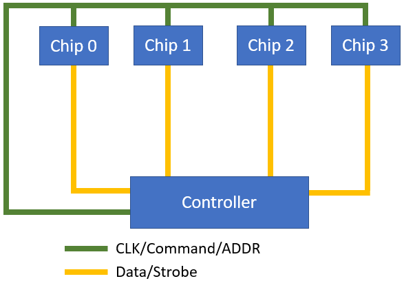
Adopt Fly-by Topology/Daisy Chain Routing for DDR4:
- Use fly-by topology or daisy chain routing methods for DDR4 memory to improve signal integrity and timing. These routing techniques help manage signal reflections and maintain proper timing relationships between signals.
Common PCB substrate materials
FR-4 (Flame Retardant 4)
- Parameters:
- Dielectric Constant: Typically between 4.0 to 4.8.
- Loss Tangent: Usually between 0.02 to 0.035.
- Water Absorption: Typically below 0.15%.
- Glass Transition Temperature (Tg): Approximately around 130°C.
- Characteristics:
- Wide Application: FR-4 is a cost-effective general-purpose PCB substrate widely used in electronics and low to medium-frequency applications.
- Good Mechanical Strength: It has high mechanical strength and wear resistance and is suitable for conventional PCB designs and manufacturing.
- Moderate High-Frequency Performance: Although its performance diminishes at higher frequencies, some high-performance variants of FR-4 can offer better high-frequency characteristics.
PTFE (Polytetrafluoroethylene, Teflon)
- Parameters:
- Dielectric Constant: Typically between 2.0 to 2.2, with very low dielectric loss.
- Loss Tangent: Extremely low, usually below 0.001.
- Water Absorption: Virtually negligible.
- Glass Transition Temperature (Tg): Not defined, as PTFE is an amorphous material without a distinct Tg.
- Characteristics:
- Excellent High-Frequency Properties: PTFE is suitable for applications in high-frequency and microwave ranges due to its low dielectric loss and tangent.
- Low Water Absorption: It is highly resistant to absorbing water, making it stable in humid environments.
- High-Temperature Resistance: Can operate reliably at temperatures above 250°C, suitable for high-temperature applications.
Rogers
- Parameters:
- Dielectric Constant: Different series of Rogers materials have varying dielectric constants, typically ranging from 2.2 to 10.
- Loss Tangent: Generally below 0.0025.
- Water Absorption: Typically below 0.03%.
- Glass Transition Temperature (Tg): Varies by series, generally above 280°C.
- Characteristics:
- Excellent High-Frequency Performance: Rogers materials are designed for high-frequency applications, featuring very low dielectric loss and tangent.
- Stable Temperature Performance: Rogers materials often have a high Tg, allowing them to maintain stability over a wider temperature range.
- Support for Complex Layer Stacking: They can be used in complex multilayer PCB designs to meet intricate circuit requirements.
When choosing materials for high-frequency PCBs, balancing performance requirements with cost considerations is essential. While advanced materials like PTFE and Rogers are favored for their low dielectric loss and stable properties at high frequencies, FR4 remains widely used in applications like PC motherboards due to its cost-effectiveness and sufficient performance for lower frequency ranges. This versatility makes FR4 a practical choice for general electronic designs where balancing performance and cost is critical.
Difference Between High-Frequency (HF) PCB and High-Speed PCB
High-Frequency (HF) PCB:
- Applications: High-Frequency PCBs are primarily used for applications involving high-frequency signals, such as wireless communication, RFID, microwave devices, and satellite communications. These applications typically operate in frequency ranges from hundreds of MHz to several GHz or even higher.
- Material Characteristics: HF PCBs utilize materials with low dielectric constant (Dk) and low dissipation factor (Df), such as PTFE (Polytetrafluoroethylene) and Rogers materials. These materials minimize signal loss and delay, ensuring signal integrity at high frequencies.
- Design Considerations: Designing HF PCBs requires specific attention to impedance matching, signal reflection, crosstalk, and electromagnetic interference (EMI) management. Routing techniques, layer stack-up, and grounding design are critical factors.
- Electrical Performance: HF PCBs emphasize stable and reliable electrical performance to ensure high-frequency signals are transmitted without interference or attenuation.
- Applications: High-Speed PCBs are used in applications requiring high-speed data transmission, such as computer motherboards, network equipment (routers and switches), data centers, and high-speed communication systems. Data rates typically range from several Gbps to tens of Gbps.
- Material Characteristics: High-Speed PCBs typically use FR4 material, but enhanced versions of FR4 or other materials may be used to improve performance. While standard FR4 has poorer high-frequency characteristics, improved variants can support high-speed data transmission to a certain extent.
- Design Considerations: Designing High-Speed PCBs focuses on signal integrity and timing control. Designers manage issues like signal reflection, crosstalk, insertion loss, return loss, and timing jitter. Factors such as trace lengths, spacing, via design, and differential pair routing are critical.
- Electrical Performance: High-Speed PCBs emphasize data transmission speed and signal integrity, ensuring high-speed signals remain accurate and stable during transmission.
Summary:
- High-Frequency (HF) PCBs prioritize signal integrity and stability in high-frequency environments, suitable for wireless communication, RF, and microwave technologies.
- High-Speed PCBs focus on signal integrity and timing control in high-speed data transmission, widely used in computer and communication equipment.
While these PCB types have distinct focuses, they may overlap in applications requiring both high-frequency and high-speed signal transmission. Therefore, comprehensive consideration of design and material selection is crucial.
Conclusion
High-frequency PCBs play a crucial role in ensuring seamless signal transmission across various applications, including telecommunications and radar systems. They are essential for achieving reliable performance in high-speed circuits and other demanding environments. Despite challenges such as signal integrity and electromagnetic interference, careful design and the use of advanced materials enable optimal functionality.
High-frequency PCBs enable innovative solutions across industries, making them a preferred choice among engineers and designers. Whether for prototypes or large-scale production, choosing the right high-frequency PCB solution is critical for ensuring performance and reliability.
For your high-frequency PCB needs, whether for prototypes or mass production, consider contacting FS PCBA for tailored PCB solutions.
Get a quote
Related Blogs
Table of Contents Drone PCB Design and Manufacturing: A Complete Guide for UAV Engineers This article was originally published in March 2024 and last updated
Table of Contents Security Camera PCBA Design Guide: Day/Night Switching and Infrared LED Driver Why Security Camera PCBA Design Matters for Day/Night Operation A security
Table of Contents AgTech Case Study: Manufacturing 2,000+ Agricultural Sensor Devices from Prototype to Production Designing an electronic prototype to large-scale production requires more than
Table of Contents Agricultural Drone PCBA Assembly: High-Power, High-Current Solutions for Farm UAVs [2026] There is growing demand for modern agricultural drones as a means
Table of Contents 2026 China PCB Manufacturer List: Top 10 PCB Suppliers & PCBA Companies in China This article was originally published in July 2022
Table of Contents Precision Agriculture – How IoT PCBA Is Transforming Modern Farming Precision agriculture is transforming modern farming by combining IoT sensors, wireless connectivity,