
Inhaltsverzeichnis
Was ist eine Leiterplatte und wie funktioniert sie?
This article was originally published in July 2022 and last updated on May 24, 2026.
PCB History: How Does Printed Circuit Board Born?

PCB Meaning: What is a Printed Circuit Board?
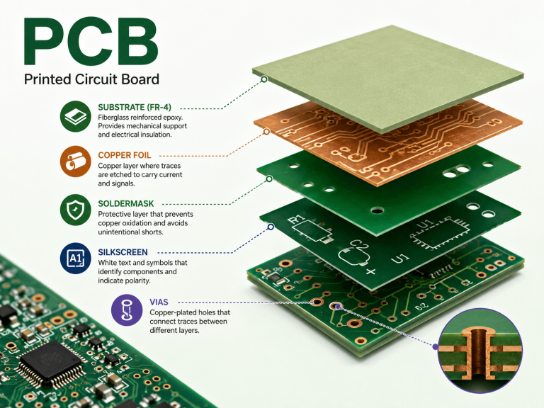
- Copper foil – it is the core of the board. From this copper layer, traces are etched to carry current and signals. Copper foil thickness is commonly indicated in ounces (oz).
- Lötstoppmaske – it is the layer usually green (but can also be blue, red, black, etc. ) covering almost all the copper except for the pads and vias. It works as a protective layer to prevent copper oxidation and to avoid unintentional shorts.
- Siebdruck – it’s the white text and symbols that identify the components (R1, C2, etc. ) and also show polarity marks.
- Vias – a small hole through the insulating layer that is copper-plated on the hole wall and copper-lined through which traces on different layers are interconnected.
PCBA Meaning: What is a Printed Circuit Board Assembly?
| PCB (Bare Board) | PCBA (Assembled Board) |
| No components | All components soldered |
| Cannot function | Fully functional when powered |
| Flat, only copper and soldermask | Populated with bulging parts |
PCB Working Principle: How Does a PCB Work?
Smartphone PCBA: An Example Shows How PCB Works

Multilayer Boards and Vias: Signal Transmission between Different Layers
- Top and bottom layers: components and some short traces, also used as antennas.
- Layer 2 & 9: solid ground and power planes.
- Layers 3–8: dense signal routing.
- Through‑hole via – goes from top to bottom, easy to manufacture, but blocks routing space on all layers.
- Blind via – connects an outer layer to one or more inner layers, without going through the whole board.
- Buried via – connects inner layers only, invisible from outside, saves surface space.

Common PCB Design Mistakes
- Large current loops – Every signal needs a return path. If the return path is long and surrounds a large area, that loop acts as an antenna, radiating noise and picking up interference. Always keep signal and return paths close together — ideally with a solid ground plane directly under the signal trace.
- Vias that shred the ground plane – Drilling a via removes copper from the ground plane. Too many vias in one area can cut the plane into pieces, forcing return currents to take long detours. This increases inductance and noise. Good designers place vias carefully and sometimes prohibit vias in sensitive regions.
- Ignoring current capacity – Copper traces have resistance. A trace that is too thin will overheat and may melt if it carries high current. A rule of thumb: 1 oz copper, 1 mm width can handle about 1 A with a reasonable temperature rise. Many hobbyist power boards smoke on first power‑up because of undersized traces. Hobbyist power boards tend to smoke on their first power-up because of underdimensioned traces.
- Crosstalk – When two parallel traces are placed too close to each other for too long a distance, there may be signal hopping between them through electric and magnetic fields. How to solve it? Increase the space between them (3 times trace width), or place a guard trace between them, grounded.
- Stress, mechanical forces, and thermal expansion – When you attach your big board by two screws only, the heat will make the board bend and crack the solder joints. You should always take into account the mounting hole positions, board dimensions, and weight of heavy parts like transformers or capacitors.
PCB Manufacturing: How to Make a Printed Circuit Board?
- Design & Output – The engineer designs the schematic and the PCB layout and then outputs the Gerber-Datei.
- Inner layer imaging – Photoresist is applied on copper-clad laminates, and the circuit design is exposed and developed.
- Ätzen – Copper that is not part of the circuit design is removed through etching.
- Kaschierung – Layers of copper-clad laminates and prepregs are joined by heat and pressure.
- Drilling & plating – Holes are drilled for the vias and lead wires and then plated with copper to create connections between the layers.
- Outer layer & soldermask – Traces on the outer layer are etched, and the solder mask is applied except the areas where there are traces and vias.
- Oberflächenbehandlung & silkscreen – Copper that is exposed from the pad is plated (ENIG: Electroless Nickel Immersion Gold). White silkscreen is applied next.
How to Check if a PCBA Board Works?
- Visuelle Kontrolle – Search for solder bridges (accidental connections), missing parts, and the correct polarity of diodes, LEDs, electrolytic capacitors, and integrated circuits. You may use a magnifying glass or a microscope.
- Resistance test – Using an ohmmeter, test the resistance between the power supply input and ground terminals. If it is close to zero (a short), do not power up your board. Locate and repair the circuit short.
- Polarization – Check whether all polarized components (LEDs, tantalum capacitors, transistors, voltage regulators) are inserted correctly according to their markings on the silkscreen layer. The same part from various lots may have different pinout schemes.
- Power-up test – Use a Stromzufuhr that has a current-limiting feature set at around 1.5 times the estimated current consumption. Power up the board and observe for 5-10 seconds. Is there any smoke or unusual smell? Are there any components heating up? If so, turn off the power immediately. Otherwise, measure the voltages across all the supply rails and ensure they are as designed.
- Function test – You can now proceed with the function test once power is stable.
What are the Different Types of Printed Circuit Boards?
- Einzelne Schicht – Copper and components on one side. Cost-effective, utilized in toys, remote controls, and calculators.
- Double Layers – Both sides used. Often used in power supplies, Arduino, and hobbyists’ boards.
- Multi-Layers (four layers and above) – Mobile phones (ten layers and above), computer motherboards (eight to twelve layers), servers (twenty layers and above), and military/aerospace applications (fifty layers and above). More layers lead to more signal integrity and high costs.
- Flexible Leiterplatte – Constructed from polyimide, making it flexible. Applications include folding phones, printer heads, and cameras.
- Aluminium-Substrat PCB – High thermal conductivity, used in LEDs and power electronics.
Fazit
Verwandte Blogs
Table of Contents PCBA Functional Testing (FCT): A Complete Guide to Ensuring Board Reliability Published on May 9, 2023 · Updated on November 6, 2026
Table of Contents IPC Class 2 vs Class 3: Acceptance Criteria, Cost Impact, and How to Choose IPC Class 2 and Class 3 are the
Table of Contents Ventilator PCB Assembly: ISO 13485, IPC Class 3 & FDA QMSR-Ready Manufacturing Published on June 24, 2022 · Updated on October 30,
Table of Contents Ventilator PCB Assembly: ISO 13485, IPC Class 3 & FDA QMSR-Ready Manufacturing How is air delivered steadily with the help of ventilators,
Table of Contents Design Rule Checking in PCB Design: From Altium DRC to SMT Assembly Published on September 10, 2024 · Updated on October 22,
Table of Contents Automotive PCB Assembly: The Complete 2026 OEM Guide Failure of a consumer good is a warranty claim. Failure of an automotive printed
Arbeiten Sie mit FS Technology zusammen und erhalten Sie professionellen PCBA-Service.